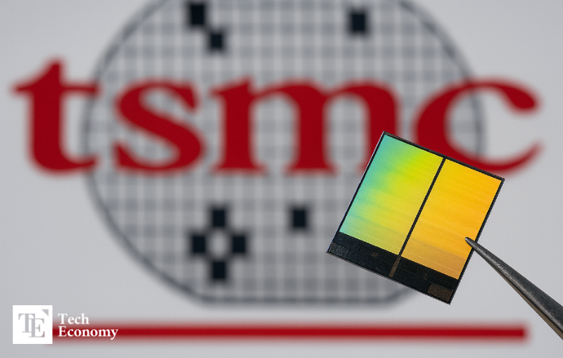
TSMC Breaks Ground on 1.4-Nanometer Semiconductor Plant, Consolidating Foundry Supremacy

Authored On
Modified
TSMC Embarks on Full-Scale Investment in Next-Generation Semiconductor Manufacturing
Mass Production in Taichung, Taiwan Set for 2028
Intel Also Signals Strong Resolve in 1.4-Nanometer Push
As TSMC officially confirmed mass production of its 1.6-nanometer process for the second half of next year, the company is also moving forward with facility investment for 1.4-nanometer production. Targeting mass production in 2028, TSMC plans to commence construction of production lines in the second half of this year. Having already widened its lead over competitors such as Samsung Electronics in processes below 3 nanometers, TSMC is now accelerating investments to secure a commanding position in the next-generation 1-nanometer-class race.
Facility Investment Begins with 2028 Mass Production Target
According to the Taipei Times on the 25th, Hsu Mao-hsin, director of the Central Taiwan Science Park Administration, stated the previous day that “TSMC will begin construction in the fourth quarter of a new 1.4-nanometer fab with a projected output value of up to $23 billion.” He added, “Everything is proceeding as planned, and TSMC is setting a detailed construction schedule and arranging contractors.”
Large local construction firms are reportedly already entering the bidding stage for the project. The site will host four semiconductor plants in total, with construction expected to take about two years. Trial production is anticipated by late 2027, followed by full-scale mass production of 1.4-nanometer semiconductors in the second half of 2028.
Hsu further projected that the new fab would generate $23 billion in output, exceeding the previously estimated $22.3 billion. The higher figure reflects the use of the more advanced 1.4-nanometer manufacturing process, beyond the 2-nanometer roadmap. Back in May, TSMC had already unveiled plans for a new facility in Taichung, known as “Fab 25,” targeting 1.4-nanometer chip production by 2028.
Industry experts view TSMC’s aggressive investments as a preemptive move to solidify its leadership in the foundry market at the 1-nanometer-class level. The company has already extended its lead in 3-nanometer and 2-nanometer processes by maintaining superior yield and stability. Its client base includes AI chip leaders such as Nvidia and AMD, as well as application processor designers like Apple and Qualcomm. According to market research firm TrendForce, TSMC commanded a 67.6% share of the global foundry market in the first quarter, compared with Samsung’s 7.7%. The gap widened from 59 percentage points in the fourth quarter of last year to 59.9 points in the first quarter of this year.
TSMC is expected to achieve mass production of 1.4-nanometer chips one to two years ahead of Samsung Electronics. Samsung, which initially aimed for 2027, has postponed its schedule to 2029, citing challenges in stabilizing yields for its 3-nanometer and 2-nanometer processes, client attrition, and sluggish orders. The company has shifted focus to enhancing its 2-nanometer technology currently in production.
Performance and Yield Secured with Existing EUV Equipment
TSMC first unveiled its 1.4-nanometer (A14) roadmap at the 2025 North America Technology Symposium in April. At the time, Kevin Zhang, senior vice president at TSMC, described the 1.4-nanometer process as “the next-generation silicon technology based on a complete process transition,” boasting up to 15% higher speed, 30% lower power consumption, and 1.23 times greater transistor density compared with 2-nanometer technology.
Of particular note was TSMC’s assertion that both its 1.6-nanometer and 1.4-nanometer processes could secure sufficient performance and yield using only existing EUV equipment. “Our technology teams found a way to produce chips at 1.4 nanometers without high-NA EUV. This is a remarkable achievement,” Zhang said. “As long as the teams continue to find solutions, there is no immediate need to adopt high-NA EUV.”
High-NA EUV lithography tools, produced by Dutch equipment maker ASML, feature a numerical aperture of 0.55, compared with the current 0.33, enabling finer patterning. While the industry had expected high-NA adoption to accelerate as process nodes shrank, widespread deployment has been delayed, largely due to cost concerns. Each high-NA machine costs about $400 million—roughly twice that of current-generation EUV systems.
“TSMC will adopt high-NA EUV only when it delivers meaningful and measurable advantages,” Zhang emphasized. “We will eventually use it, but only when it maximizes profit and return on investment.” TSMC, which already operates the largest fleet of conventional EUV tools, is leveraging techniques such as multi-patterning to maintain flexibility in its adoption timeline.

Intel Also Bets on 1.4 Nanometers
Intel is likewise positioning its 1.4-nanometer process as a strategic lever for regaining leadership in semiconductor manufacturing. At Citi’s Global TMT Conference in New York on September 5, CFO Dave Zinsner said, “By next year, progress on the 1.4-nanometer process will be clearly visible.”
At Goldman Sachs’ Communacopia & Technology Conference in San Francisco on September 8, Intel vice president of corporate relations John Pitzer added that the company was “actively collaborating with potential external clients in the development of the Intel 14A process.” Unlike the 18A process, which was primarily tailored for internal products, the 14A process has been designed from the outset to incorporate external client requirements.
Pitzer explained that semiconductor process development proceeds through three stages: definition, development, and mass production. While all decisions regarding 18A were optimized for Intel’s own products, he stressed that the 14A process, currently in the definition stage, is being shaped in active collaboration with external clients. “We are receiving earlier, more extensive, and higher-quality feedback than before,” he said, adding that Intel plans to finalize key decisions on 14A in the second half of next year to align with client production needs.
The success of the 1.4-nanometer process is widely regarded as central to Intel’s turnaround strategy. Last July, Intel announced a sweeping restructuring plan, making clear that the expansion of 1.4-nanometer production would hinge on secured customer orders. At the time, CEO Pat Gelsinger’s remarks sparked concerns that any delay in the 1.4-nanometer project could signal Intel’s retreat from the race for process leadership.
Similar Post