Surging AI Demand Drives TSMC’s Node Expansion — Samsung and Intel Escalate Their 2nm Challenge

Authored On
Modified
TSMC CEO: “Market Demand Is Far Beyond What We Can Handle”
Company Plans to Expand Leading-Edge 2nm Fabs From Seven to Ten to Meet Demand
Samsung and Intel Raise Their 2nm Capabilities, Setting Up a Direct Challenge to TSMC
Global foundry leader TSMC has acknowledged a shortage in chip production capacity. As the AI market expands rapidly and demand for high-performance chips surges, orders have concentrated at TSMC—the most reliable producer of advanced chips—creating a bottleneck in supply. To keep pace with demand, TSMC is moving ahead with aggressive capacity expansion, while rivals Samsung and Intel are boosting their own leading-edge capabilities in an effort to capture the overflow.
TSMC-Driven Chip Bottleneck
According to the semiconductor industry on the 26th, TSMC CEO C.C. Wei said at a Semiconductor Industry Association awards event that “current demand is three times higher than what we can produce.” His remarks indicate that orders flooding into TSMC have reached a “tsunami” level. Traditional processor giants like NVIDIA, AMD, and Intel—as well as ASIC makers such as Broadcom and Marvell—are all directing massive orders to TSMC. But with insufficient capacity, TSMC has effectively admitted it cannot keep up.
The core reason behind this imbalance is TSMC’s dominance in leading-edge manufacturing. Most of the high-performance and AI chips now in explosive demand are produced using TSMC’s advanced nodes. Intel and Samsung Foundry are offering alternatives, but according to analyses from outlets such as WCCFTech, the only processes that have actually reached mass production during the current AI boom are TSMC’s.
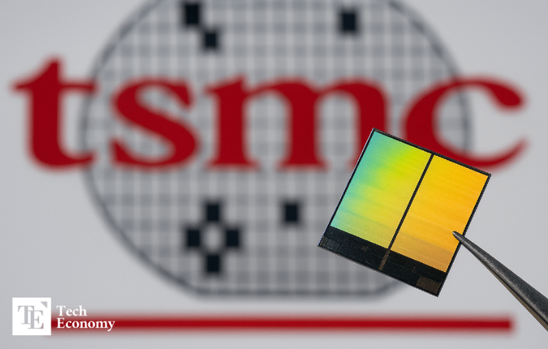
Confidence in TSMC’s cutting-edge 2-nanometer (N2) technology remains particularly strong. Regardless of technical debates, major customers prefer TSMC because its yields and volume production are proven—fueling the bottleneck. Allocation practices are intensifying the squeeze as well. A significant share of TSMC’s total capacity is already locked in by long-term contracts with top customers such as NVIDIA and Apple. Smaller fabless companies and later entrants are left waiting indefinitely for production slots. In effect, the entire AI ecosystem is captive to TSMC’s production schedule.
TSMC Expands 2nm Capacity to Meet Surging Demand
TSMC plans to expand its 2-nanometer production footprint to keep up with market demand. According to Taiwan’s Liberty Times on the 25th, the company told government agencies—including the National Science and Technology Council (NSTC)—that it intends to build three additional 2nm fabs in Taiwan. The sites are expected to be located in Tainan’s Southern Taiwan Science Park, with total investment estimated at $4.21 billion. The report noted that the project covers 40 hectares and could break ground as early as next year.
Industry observers say TSMC’s expansion was widely expected. The company had already announced during its third-quarter earnings call last month that it plans $40–42 billion in capital expenditures this year to respond to soaring AI demand. CFO Wendell Huang said about 70% of that spending will go toward advanced process technologies, 10–20% toward specialty technologies, and the remaining 10% toward advanced packaging, photomasks, and other projects.
If this trajectory continues, analysts expect TSMC’s monthly 2nm wafer output to reach 80,000–90,000 wafers by the end of next year—roughly double the current level of 40,000. By 2027–2028, 2nm technology is expected to become as mainstream as 3nm is today, while TSMC’s A16 (1.6nm) process—scheduled for mass production in 2028—is projected to become the company’s next major node.
Global Battle for 2nm Leadership Intensifies
Competitors are strengthening their 2nm capabilities to challenge TSMC’s dominance. Samsung is viewed as having a generational edge in gate-all-around (GAA) architecture. Both Samsung and TSMC use GAA at 2nm, but Samsung adopted it first at the 3nm node—the earliest in the world. GAA reduces leakage and significantly improves performance and power efficiency compared with FinFET, giving Samsung valuable experience and a key competitive advantage.
Pricing is another important factor. While TSMC is reportedly planning a 10–20% increase in 2nm wafer prices, Samsung is winning customers with a more flexible pricing strategy. Tesla has diversified production of its next-generation AI5 automotive chip across both TSMC and Samsung, and has awarded its multibillion-dollar AI6 contract entirely to Samsung. Even so, Samsung continues to trail in yields. The company is now believed to have raised its 2nm yields to the 50–60% range—significant progress from roughly 30% in the past, but still short of TSMC’s reported 80%.
Intel, a late entrant in the foundry race, is rebuilding with strong backing from the U.S. government and industry. NVIDIA has invested $5 billion in Intel, and the U.S. government has acquired a 10% stake, in effect moving Intel closer to a state-backed enterprise. The Trump administration’s “support domestic champions” stance has helped lay the groundwork for Intel’s recovery.
Intel’s foundry technology is also making steady gains. At the RBC Capital Markets Global TMT Conference on the 18th, Intel said yields for its 18A process have been improving by 7% each month over the past seven to eight months. If the trend continues, the company expects to mass-produce Panther Lake based on 18A without additional cost overruns. The 18A node—Intel’s 1.8nm-class process—is designed to compete directly with the 2nm-class technologies of TSMC and Samsung.
Similar Post