China’s Chip-Stacking Move That Breached the U.S. 14-Nanometer Blockade Blurs the Line Between Technology and Cost

Authored On
Modified
A short-term push to catch up to 4-nanometer nodes gathers momentum
Tighter U.S. controls emerge as a new variable in the technology race
Rapid catch-up expected despite thermal and yield constraints
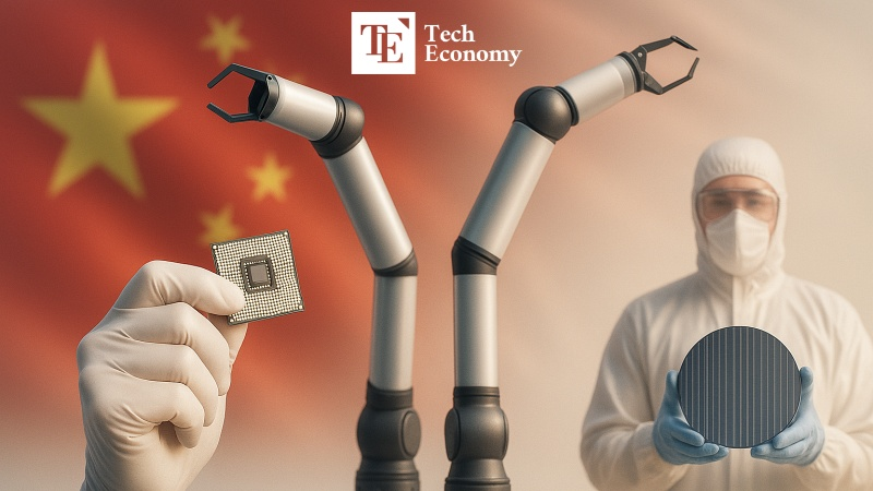
China’s claim that it has achieved 4-nanometer-class performance by stacking chips made on legacy process nodes has sent ripples through the global semiconductor market. Beijing’s attempt to boost performance without access to the latest manufacturing technologies is colliding with Washington’s tightening export controls, amplifying the impact. While industry players point to fundamental limits such as heat dissipation and stability, many still expect China’s characteristic rapid catch-up to play out once again.
A complete break from foreign technology
According to IT outlet DigiTimes on the 26th (local time), Wei Shaojun, vice chairman of the China Semiconductor Industry Association and professor at Tsinghua University’s Department of Integrated Circuits, attended the recent ICC Global CEO Summit and unveiled China’s strategy for next-generation AI semiconductors. He said China had achieved performance comparable to Nvidia’s latest chips by vertically stacking legacy 14-nanometer chips using a technique known as 3D hybrid bonding. He further claimed that this design had moved beyond the experimental stage and reached functional maturity.
The industry has focused on the fact that China has now effectively formalized a strategy to close the performance gap using only its own mature-node processes, given that it cannot compete head-on in advanced-node scaling. The move is being framed as a breakthrough achieved under strict U.S. export controls on advanced equipment. Wei described 3D hybrid bonding not as mere packaging but as an alternative architecture that eliminates bottlenecks by minimizing data-transfer distance between memory and logic, repeatedly asserting that it can completely eliminate reliance on external technologies.
To support his argument, Wei also laid out specific technical components. First is a software-defined logic structure that allows the operation of logic chips to be flexibly optimized depending on workload and conditions. Second is near-memory computing, an approach that tightly integrates memory and compute units in a three-dimensional configuration to minimize latency. Third is the use of 3D hybrid bonding technology to physically connect logic and DRAM. He said this combination can fundamentally relieve bandwidth constraints inherent in conventional general-purpose GPU (GPGPU) architectures.
Wei went on to say that the new design delivers 120 teraflops (TFLOPS, where 1 TFLOPS equals one trillion operations per second) of performance and power efficiency of 2 TFLOPS per watt, once again underscoring China’s semiconductor roadmap to boost performance through innovation in design, placement, and stacking. However, the fact that these figures were presented without any physical demonstration has sparked controversy both inside and outside China. Many in the industry believe the announcement was less about proving raw performance and more about sending a strategic message that China can pursue alternative paths around U.S. export barriers on advanced process nodes.
Will this undermine controls on mature chips?
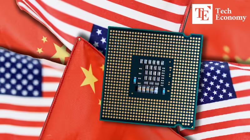
The news has also drawn renewed attention to a U.S. measure announced earlier this year that requires prior scrutiny of customers when selling chips at 14 nanometers and below. The measure traces back to a draft executive order from the Biden administration, introduced under the banner of preventing a recurrence of incidents in which chips made by TSMC were diverted and ended up in Huawei products. Washington confirmed that existing rules targeting 7-nanometer and below were insufficient to completely block China’s procurement channels. It therefore expanded pre-approval requirements to wider process ranges such as 14-nanometer and 16-nanometer, and began demanding detailed verification of customer identity and actual end-use before any sale.
At the same time, the United States barred AI semiconductor purchases entirely for 20 countries including China, Russia, Iran, and Iraq, and mandated government approval for sales of mature-node chips to most countries other than 18 designated allies. Foundries were required to assess everything from their customers’ ownership structure and final packaging locations to the number of transistors on each chip, with 30 billion transistors used as a key threshold. Chips that did not satisfy these conditions were treated as controlled items regardless of whether they were advanced or mature products. Washington sought to shut down, in one sweep, all channels involving third-country procurement, disguised orders, and supply-chain leakage at the packaging stage.
At the time, global industry opinion largely held that Washington’s measures were excessive. But China’s recent experiments stacking 14-nanometer and 18-nanometer chips have led to a reassessment of the U.S. approach. Mature nodes are generally characterized by lower manufacturing costs, extensive installed capacity, and faster iteration cycles for experimentation. From the U.S. perspective, such an environment naturally raises the risk that China could use mature processes as a platform for new types of performance gains. That concern aligns closely with the present reality in which 14-nanometer chips have become the foundation for exploring new computing architectures.
Rising potential for low-cost market expansion
Thermal management is widely regarded as the key challenge China must solve before its 3D hybrid bonding approach can be realized in commercial products. Vertically combining 14-nanometer logic with 18-nanometer DRAM is effective for improving performance by shortening data-transfer distances, but as the number of process layers grows, baseline power consumption increases and heat density escalates exponentially. If heat cannot be contained, yields become unattainable, directly driving up unit costs. The performance numbers China has presented may indicate technological potential, but ongoing concerns about reliability and yield highlight the practical constraints that still stand in the way.
Even so, the industry believes China has a strong chance of rapidly improving its stacking technology, given how quickly it caught up in DDR4 and DDR5. CXMT, for example, unveiled DDR5 and LPDDR5X products at an official exhibition in just 11 months, rapidly shifting from a DDR4-focused strategy to a premium lineup. At the time, many observers concluded that CXMT had pushed its entire roadmap close to global standards. With such rapid catch-up cases repeating among Chinese memory companies, many expect a similar speed-driven pursuit in stacking-based AI chips.
Chinese DRAM makers are also accelerating technology upgrades and line expansions by hiring large numbers of experienced engineers from South Korea and Japan. CXMT’s current monthly wafer input is 270,000, roughly half that of Samsung Electronics and SK Hynix, but the company is quickly building up quality verification and mass-production experience through its domestic market. This pace of scaling, coupled with its engineering base, is expected to help tackle stability challenges associated with stacking technologies. China’s practice of using its domestic market as a testing ground also enables rapid iteration and verification, further accelerating its catch-up trajectory.
Moreover, the low-cost structure inherent in mature-node manufacturing is expected to play a crucial role in helping Chinese firms gain market share. The lack of EUV equipment is a clear handicap in the race below 10 nanometers, but if 3D stacking and DRAM-stacking roadmaps gain traction, China will have more room to compete on cost-adjusted performance rather than pure miniaturization. When such cost advantages combine with government subsidies and other forms of support for capacity expansion, expectations are growing that Chinese companies will quickly seize the low-end segment and expand their influence across the global supply chain.
Similar Post