Elon Musk Declares “We Will Break the Chip Wall,” Tesla Moves Toward Semiconductor Self-Reliance With ‘Terafab’

Authored On
Modified
Blueprint for In-House Chip Production to Move Beyond Outsourced Manufacturing
Cost Strategy Activated Amid Expectations of Prolonged Semiconductor Bottlenecks
U.S. Government Push to Expand Domestic Semiconductor Manufacturing Base
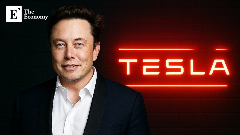
Tesla Chief Executive Officer Elon Musk has formally outlined plans to produce artificial intelligence semiconductors directly, signaling the launch of the company’s in-house semiconductor manufacturing facility project known as “Terafab.” He emphasized the need for internal production, warning that semiconductor supply constraints could persist for years as artificial intelligence adoption expands worldwide. The plan is also being discussed against the backdrop of U.S. policy efforts to expand domestic semiconductor manufacturing capacity and a broader trend of global companies increasing local production investments.
Challenges Expected in Securing Process Technology
On the 14th, Musk announced on his social media platform X the previous day that “the Terafab project will launch in seven days.” Terafab is a semiconductor manufacturing facility whose necessity Musk has repeatedly highlighted in shareholder meetings and conference calls. At Tesla’s annual shareholder meeting last November, he first revealed the concept, stating that “even assuming the best-case production scenarios from partners such as Samsung Electronics, TSMC, and Micron, it is still insufficient to meet demand for Full Self-Driving (FSD) systems and humanoid robots.”
Tesla currently maintains a model in which it designs artificial intelligence chips internally—including the AI4 chips used in electric vehicles and the Optimus humanoid robot—while outsourcing manufacturing to foundries such as TSMC and Samsung Electronics. Under this structure, semiconductor design capabilities are developed internally while fabrication processes are handled by external foundry companies. Although this model is widely used across the global semiconductor industry, Tesla’s move toward building its own semiconductor manufacturing facility is expected to mark a major shift. In January, Musk also remarked that “people underestimate geopolitical risk factors that will become major issues within a few years.”
Musk also suggested that Terafab’s production capacity could surpass existing foundry facilities. According to his explanation, Terafab aims for production capabilities larger than TSMC’s “Gigafab,” which produces 100,000 wafers per month. Musk has long adhered to a principle of manufacturing components internally when the “Idiot Index”—a measure comparing the price of a finished product to the cost of its raw materials—exceeds 10, and semiconductor manufacturing is now being evaluated under that same principle. He has also left open the possibility of cooperation with Intel in building an AI chip factory.
Industry observers, however, largely point to the technological difficulty of Tesla entering the semiconductor manufacturing market. Nvidia Chief Executive Officer Jensen Huang commented on the issue in November last year, shortly after Musk revealed the Terafab concept, during a TSMC event, stating that “reaching the level of engineering, scientific, and artistic mastery that TSMC represents is extraordinarily difficult.” Because the foundry industry requires decades of accumulated process technology and operational expertise, the broader industry view holds that Tesla’s plan for in-house semiconductor production is unlikely to materialize immediately.
Supply Imbalances Likely to Persist
Despite these skeptical views, Tesla’s urgency in advancing Terafab stems from the belief that semiconductor shortages will not be resolved quickly. Musk described this challenge using the phrase “chip wall.” In a podcast appearance, he said, “If we do not build factories, we will hit the chip wall,” adding that “there are only two options: hit the chip wall or build factories.” In the AI industry, semiconductors ultimately determine computing capacity, meaning supply constraints could directly limit the pace of technological development.
Terafab, as envisioned by Tesla, represents a direct response to this bottleneck. If the company continues relying entirely on external foundries, AI chip supply will inevitably remain dependent on external production schedules. By securing its own manufacturing facilities, Tesla expects to stabilize supply while simultaneously managing cost structures. Some analysts also argue that Tesla believes competitiveness can be achieved through process optimization and manufacturing efficiency rather than purely through chip design competition. Concentrating early investments on equipment and recruiting core engineering talent could allow production systems to be established relatively quickly.
Tesla’s talent acquisition strategy has already moved into the execution phase. Musk posted on X that “if you want to stay in Korea and work in chip design, manufacturing, and AI software, join Tesla,” accompanied by a South Korean flag emoji. Tesla Korea likewise stated in a job posting for AI chip design engineers that it is “seeking talent to develop the world’s highest-volume AI chips,” explaining that the project aims to create “an AI chip architecture with the highest production volume in the world.” Applicants are asked to present the three most difficult technical problems they have solved, a requirement interpreted as emphasizing practical design and verification experience.
Building a U.S. Design-Manufacturing-Packaging Supply Chain
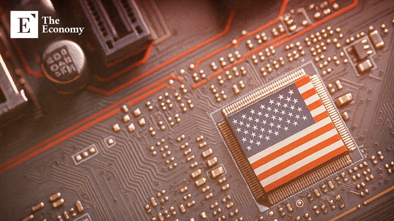
Tesla’s Terafab initiative has gained additional momentum from policy conditions supporting semiconductor self-reliance in the United States. Following a series of events—including technological competition with China, supply chain vulnerabilities, and shortages of automotive semiconductors during the COVID-19 pandemic—the United States concluded that design leadership alone could not guarantee economic security. Washington has therefore concentrated significant funding and institutional support on reshoring and onshoring semiconductor manufacturing capacity back to U.S. territory. The strategy reflects a long-term effort to absorb demand for critical chips domestically while securing control over procurement during crises.
In August 2022, the United States enacted the CHIPS and Science Act, committing $52.7 billion in subsidies and tax incentives. At the same time, TSMC’s investment in Arizona expanded from $12 billion to $65 billion, and in March last year the company proposed an additional $100 billion investment alongside plans to construct five new facilities. In addition, Intel announced plans to invest $28 billion in Ohio, while Micron unveiled plans to invest $100 billion in New York to build memory fabrication plants.
These developments reflect the emerging supply chain dynamics of the AI era, in which the United States aims to anchor wafer production, advanced packaging, and memory back-end processes within its own territory. Establishing an end-to-end supply chain linking design, manufacturing, and packaging allows semiconductor production for AI data centers and other high-value strategic chips to achieve three simultaneous effects: production closer to customers, shorter delivery times, and diversification of geopolitical risk. The massive “Stargate” data center project, being pursued by OpenAI and Oracle with roughly $500 billion in investment across the United States, illustrates this concentration of demand. Tesla’s Terafab concept can be understood within the same context of the United States reshaping semiconductor manufacturing bases domestically.
Cost and labor challenges are often cited as weaknesses in the revival of U.S. manufacturing. According to semiconductor cleanroom construction firm Exyte, building a fabrication plant in the United States takes an average of 38 months—nearly twice as long as the 20 months required for a cutting-edge facility in Taiwan. Nevertheless, government subsidies and tax credits are being used to bridge the so-called “cost gap,” while more than 25,000 new jobs have been created in Arizona alone since 2020. This trend indicates that market participants have placed considerable confidence in the continuity of policy support and the concentration of demand. In such an environment, companies with large internal demand for AI chips have stronger incentives to consider bringing manufacturing in-house. This helps explain why Tesla’s Terafab initiative is increasingly interpreted as an industrial choice aligned with the broader U.S. strategy for semiconductor self-reliance.
Similar Post