"Too Early to Catch Up with TSMC and Samsung Electronics" — China’s Struggling Advanced Semiconductor Yields Signal Need to Build Fundamentals in Mature Nodes

As one of the youngest members of the team, Tyler Hansbrough is a rising star in financial journalism. His fresh perspective and analytical approach bring a modern edge to business reporting. Whether he’s covering stock market trends or dissecting corporate earnings, his sharp insights resonate with the new generation of investors.
Authored On
Modified
China’s advanced process capabilities remain inadequate despite massive investment
TSMC and Samsung Electronics push ahead in leading-edge race with rising 2nm yields
“Target niche markets” — Chinese firms dig into mature process segments
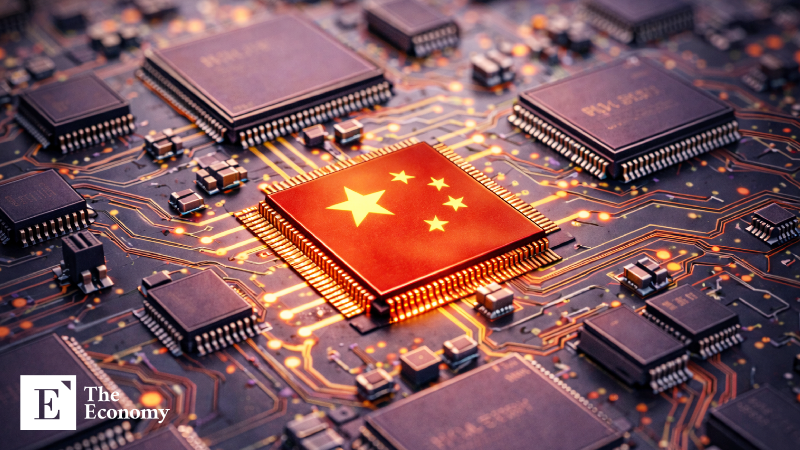
China’s semiconductor industry is facing persistent difficulties in improving yields (the proportion of defect-free chips) in advanced manufacturing processes. Despite the injection of astronomical subsidies into the sector over the past decade, the country has yet to meaningfully narrow the technological gap with leading nations such as South Korea and Taiwan. Market observers argue that China must first strengthen its foundational capabilities in mature nodes before attempting to compete at the cutting edge.
Sluggish Qualitative Growth in China’s Semiconductor Sector
According to a report released on the 15th (local time) by the Center for Strategic and International Studies (CSIS), China invested approximately $142 billion in semiconductor policies between 2014 and 2023. This figure far exceeds the $39 billion pledged by the United States over the same period. Such aggressive investment has translated into visible expansion in scale for Chinese semiconductor firms. For instance, SMIC (Semiconductor Manufacturing International Corporation), China’s largest foundry, ranked third globally for the first time in the first quarter of 2024 and has since maintained a market share of around 5%–6%, rapidly closing in on second-place Samsung Electronics.
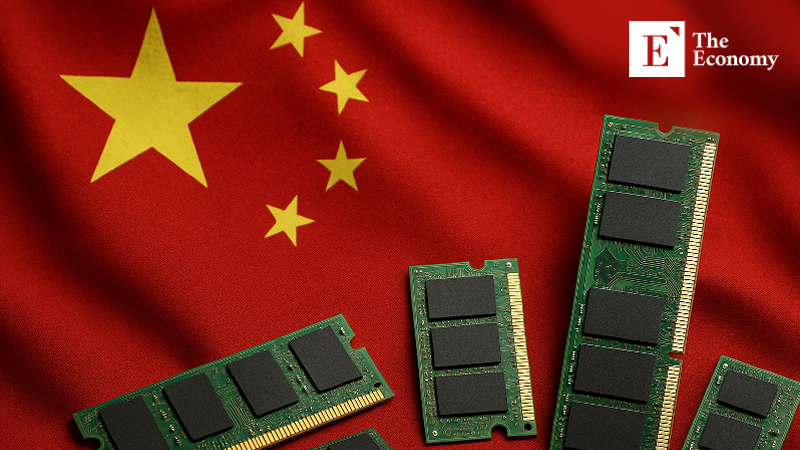
China’s semiconductor self-sufficiency rate is also steadily rising. In a report released last month, Morgan Stanley noted that “Chinese semiconductor firms are gradually reducing their reliance on TSMC in advanced process technologies,” and projected that China could achieve a self-sufficiency rate of 76% in the artificial intelligence (AI) graphics processing unit (GPU) market by 2030. This reflects the cumulative impact of government efforts to nurture domestic players such as Huawei, Alibaba, Cambricon, and Moore Threads.
However, qualitative growth in China’s semiconductor industry remains constrained. SMIC’s 5-nanometer (nm) process yield is reportedly only around 20%. U.S. sanctions have blocked imports of extreme ultraviolet (EUV) lithography equipment, which is exclusively supplied by the Netherlands’ ASML, thereby delaying progress in advanced process development. Currently, SMIC and others are known to rely on older deep ultraviolet (DUV) equipment, employing a “multi-patterning” technique that repeatedly overlays circuit patterns. A market expert noted, “Advanced processes using DUV are 40%–50% more expensive than EUV-based processes,” adding, “With yield improvement also difficult, achieving profitability through large-scale commercial production is extremely challenging.”
Frontline Competition in the Global Market
The yield challenges faced by China’s semiconductor industry become even more apparent when compared to TSMC and Samsung Electronics, which are competing at the forefront of the global market. TSMC’s 2-nanometer (N2) process yield stood at around 60% during initial trial production and has since entered a stabilization phase, rising to approximately 70%–80% following mass production at the end of last year. This level meets or exceeds typical thresholds for commercial mass production. TSMC aims to achieve an 80% yield in its enhanced N2P process.
Samsung Electronics has also made significant progress. Its 2-nanometer (SF2) process yield, which remained in the 20% range in the second half of last year, has recently climbed to around 55%. Through its next-generation Gate-All-Around (GAA) transistor architecture, Samsung has improved power efficiency by 8% and reduced chip area by 5% compared to previous processes, enhancing overall technological maturity. This has translated into stronger momentum in securing global clients. In July last year, Tesla signed a $16.5 billion contract with Samsung Electronics for the foundry production of next-generation AI6 chips, while Qualcomm has also formalized its collaboration with Samsung as part of supply chain diversification efforts. Samsung expects its 2-nanometer order volume to increase by more than 30% this year compared to the previous year.
Amid these developments, Samsung is reportedly advancing its target timeline for turning its foundry business profitable from 2027 to this year. The division had previously struggled with low yields in advanced processes, leading to weak order intake and multi-billion-dollar losses since 2023. However, conditions have shifted as advanced processes stabilize and demand and utilization rates for mature nodes increase. Looking ahead, Samsung aims to improve profitability and achieve a 20% market share in foundry revenue by 2027.
Huahong and SMIC Move into 7nm
The market widely believes that Chinese semiconductor firms will find it difficult to compete with TSMC and Samsung Electronics in leading-edge processes in the near term. Rather than continuing to pour resources into underperforming 5-nanometer technologies, analysts argue that building core capabilities in lower nodes is a more viable strategy. Indeed, some Chinese companies are already targeting such opportunities. A representative case is Huahong Semiconductor, China’s second-largest and the world’s sixth-largest foundry. According to reports by Reuters and other media last month, Huahong’s affiliate Huali Microelectronics has recently developed 7-nanometer process technology and begun preparations for its adoption.
Reuters reported that Huali could secure production capacity of several thousand 7-nanometer wafers per month by the end of this year. However, specific details such as yield rates have not yet been disclosed. Until now, Huahong Semiconductor has achieved revenue growth by focusing on mature processes of 28 nanometers and above. Last year, its revenue reached $2.4021 billion, up 19.9% from $2.004 billion the previous year, while its gross margin rose by 1.6 percentage points to 11.8%. If Huahong successfully establishes competitiveness in 7-nanometer foundry processes, it could more rapidly capture niche segments in the market while TSMC and Samsung Electronics remain focused on leading-edge competition.
SMIC is also operating a 7-nanometer foundry process. This node is considered effectively the most advanced process available domestically in China, and chips produced through it are already being applied in smartphone application processors (APs) and certain AI chips. Recently, expansion of production lines and increased output of 7-nanometer products have been underway. However, the process remains limited to a restricted mass production structure centered on specific clients. The primary demand comes from AP and AI chips designed by HiSilicon, Huawei’s fabless semiconductor subsidiary.
As one of the youngest members of the team, Tyler Hansbrough is a rising star in financial journalism. His fresh perspective and analytical approach bring a modern edge to business reporting. Whether he’s covering stock market trends or dissecting corporate earnings, his sharp insights resonate with the new generation of investors.
- Previous [AI Bubble] “Even Taking on Credit Risk”: SoftBank Goes All-In on AI Investment, With OpenAI’s IPO Likely to Determine the Outcome
- Next [U.S.-Iran War] The U.S. and Iran Return to the Negotiating Table Under Economic Duress, but Divergence Over Nuclear Concessions and Trump’s ‘Top-Down Diplomacy’ Remain Variables
Similar Post