TSMC Maximizes “Monopoly Profits” Through 2nm Price Hike, While Samsung and Intel Need Time to Catch Up

Authored On
Modified
Dominant position turns into pricing power
Yield stability drives overwhelming order intake for TSMC
Monopoly structure continues to erode industry profitability
TSMC, the world’s largest contract chipmaker, has strengthened its market dominance by sharply raising prices for its next-generation process nodes. Backed by stable yields and a clear technological lead, TSMC’s premium pricing policy has further burdened major clients such as Qualcomm and MediaTek, while rivals Samsung Electronics and Intel remain constrained by lengthy customer qualification steps. As higher foundry prices ripple through to end products, the industry faces a cycle of weakening profitability. Meanwhile, TSMC has already moved up the construction schedule for its 1.4-nanometer fabs, solidifying its “ultra-gap” advantage. Observers warn that the global semiconductor industry’s monopoly structure is likely to deepen further.
Major Clients Struggle as Price Hike Becomes Reality
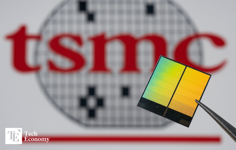
According to industry sources on the 16th, TSMC plans to raise the price of its 2nm wafer by about 50 percent compared to the previous generation. Although the increase had been hinted at since September, the magnitude of the hike has stirred unease throughout the market. The price for TSMC’s 3nm process already exceeds 20,000 dollars per wafer, but the 2nm process is expected to reach around 30,000 dollars. This is nearly triple the 10,000-dollar price level of the 7nm era in 2018, marking a seismic shift in the cost structure of the semiconductor industry.
The industry views TSMC’s high-price strategy as rooted in its monopolistic technological advantage. With each extreme ultraviolet (EUV) lithography machine costing hundreds of millions of dollars, the company’s annual investment in research and development and new fabs runs into tens of billions. Passing those costs to customers has become part of TSMC’s business model, underpinned by a technological lead that few competitors can match. Currently, only TSMC, Samsung, and Intel can mass-produce chips below 3nm, but TSMC’s superiority in yield and reliability gives it unmatched pricing power.
The first to feel the pinch are TSMC’s key clients. Qualcomm and MediaTek are expected to see production costs rise by 16 percent and 24 percent, respectively, which will inevitably translate into higher retail prices for end products. Analysts project that CPU and GPU prices could jump about 30 percent, with products once priced at 300 dollars likely rising to around 400 dollars. Qualcomm, which depends heavily on TSMC, is now reportedly considering renegotiating its foundry contracts.
Of note, TSMC has opted to raise production costs despite facing workforce shortages and equipment optimization issues at its Arizona plant, aiming to maintain domestic-level yields there. This move appears less about offsetting losses and more about protecting its technological leadership through a “price premium.” Such actions are reshaping the global semiconductor competition from a technology-driven race into one defined by profitability. As one industry observer put it, “Each new node now comes with a built-in price premium—technology is no longer the power, price is.”
Samsung and Intel Struggle to Seize Opportunity Amid Yield Gaps
Some analysts argue that TSMC’s 2nm price hike could actually present an opportunity for followers like Samsung and Intel. As cutting-edge process costs soar, firms with stronger cost competitiveness could gain new contracts. Samsung, in particular, is pursuing a price-cut strategy that contrasts sharply with TSMC’s premium pricing. The company recently offered major clients a 2nm wafer price of around 20,000 dollars—over 30 percent lower than TSMC’s expected 30,000-dollar rate. Samsung’s yield has improved from about 30 percent early this year to 40–50 percent, while performance has risen 12 percent and power efficiency roughly 25 percent compared to its 3nm process. For cost-sensitive clients, Samsung’s approach could emerge as a practical alternative.
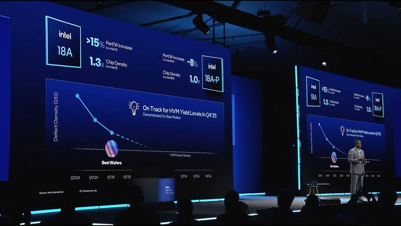
Intel, meanwhile, has begun production of its 18A (2nm-class) process, marking its re-entry into advanced foundry competition. The company has started manufacturing client chips codenamed “Panther Lake” at its Fab 52 facility in Arizona, with full-scale supply slated for January next year, alongside the server-grade “Xeon 6 + Clearwater Forest.” These efforts are part of Intel’s broader plan to restore its vertically integrated supply chain—design, manufacturing, and packaging—through a 100-billion-dollar investment drive. With support from the U.S. government and tech giants such as SoftBank and NVIDIA, Intel is leveraging both financial and policy advantages to win back clients that prefer North American production bases.
However, reality remains challenging. Industry estimates put TSMC’s current 2nm yield at 60–70 percent, with mass production expected to reach 90 percent. Shipments of 100,000 wafers per month will begin by the end of this year, and next year’s capacity is already fully booked. Despite its high prices, TSMC’s stable yields continue to secure client confidence. For customers, switching foundries entails additional costs for design verification, compatibility testing, and re-packaging, making it difficult to break away from TSMC’s grip. The consensus across the industry is that the company’s monopoly is sustained by trust and performance rather than price alone.
Ultimately, Samsung and Intel’s greatest challenge is yield verification. Foundry contracts typically require a series of steps—customer samples (CS), quality testing, feedback incorporation, engineering samples (ES), and internal certification—before final approval. This process takes six to nine months on average, and failed verification can lead to millions in rework costs. Samsung has provided 2nm Gate-All-Around (GAA) process samples for mobile application processors to clients such as Qualcomm, but still faces obstacles in mass-production stability and packaging compatibility. Opportunities do exist, yet expanding market share will take considerable time.
Profit Pressure Spreads Across Vendors and Materials Sectors
The impact of TSMC’s price hikes extends well beyond the foundry sector. The monopoly built on its yield advantage and technological lead is reshaping market dynamics, straining profitability across the entire semiconductor value chain. Rising wafer prices push up costs for device manufacturers and consumers alike, with the burden cascading through CPUs, GPUs, and other system semiconductors. Given the industry’s high fixed costs, increased prices directly squeeze profit margins for equipment and materials vendors.
This situation stems from TSMC’s dominant position. The gap in advanced process technology has evolved beyond simple competition into a matter of supply-chain reliability. Supported by long-established design support infrastructure, supplier networks, and procurement priority with equipment vendors, TSMC has minimized transition risks that still plague competitors. By contrast, Samsung and Intel remain exposed to fluctuations in yield, supply bottlenecks, and packaging issues. Industry experts note that TSMC’s advantage arises not merely from technology, but from its integrated operational efficiency spanning manufacturing, procurement, packaging, and human resources.
At the same time, global capital flows and investment strategies are increasingly orbiting around TSMC. Intel’s attempts at resurgence—backed by U.S. government funding and major IT investors such as NVIDIA and SoftBank—have yet to dislodge TSMC’s grip on the supply chain. The U.S. government’s incentives to boost domestic production paradoxically depend on TSMC’s Arizona fabs, highlighting the company’s entrenched influence. As a result, pricing power and profit distribution in the foundry market are becoming even more concentrated in TSMC’s hands.
TSMC is now moving ahead with construction of its next-generation 1.4nm (A14) fabs to further expand its lead. The company plans to install more than 30 EUV lithography machines at its new Taichung facility, targeting mass production in the second half of 2028, with similar processes planned for its Hsinchu and Kaohsiung sites. While the A14 process promises major improvements in performance and power efficiency over 2nm, it also poses tougher cost and yield challenges. Nevertheless, TSMC’s accelerated construction and early workforce recruitment suggest its ambition to dominate not only technology and supply chains but also capital and policy environments.
Similar Post