Samsung Declares “Foundry Comeback” — Can 70% Yield in 2nm GAA Process Close the Gap with TSMC?

Authored On
Modified
Exynos 2600 mass production signals a revival
Yield and cost war with TSMC intensifies
GAA technology boosts efficiency in 2nm race
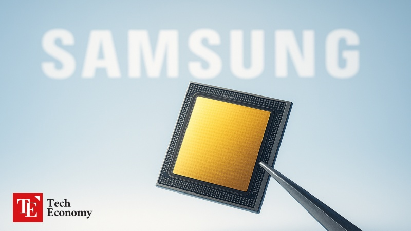
Samsung Electronics has declared a full-scale comeback in its foundry business, raising its 2-nanometer yield target to 70 percent—a move that underscores growing confidence in its manufacturing competitiveness. As rival TSMC dominates the global foundry market with a high-yield, premium-pricing strategy, Samsung aims to regain ground with more affordable pricing and advanced Gate-All-Around (GAA) transistor technology. The company’s recent “2nm optimism,” presented during a presidential office meeting, reflects this strengthened technological confidence. Industry observers say the year-end yield results will serve as a turning point for the global foundry hierarchy.
2nm process: the ultimate test of market confidence
According to industry sources on the 23rd, Kim Yong-beom, policy chief at South Korea’s presidential office, recently convened a semiconductor strategy meeting attended by top executives from Samsung Electronics, SK Hynix, major equipment suppliers, and academic experts. The meeting focused on how Korean companies are responding to the global supply chain realignment and competing with Taiwan’s TSMC in the foundry sector.
At the meeting, Samsung CTO and Device Solutions (DS) division head Song Jae-hyuk reportedly stated, “Our 2-nanometer process is progressing smoothly, and we are close to reclaiming the No. 1 position in global foundries.” His remarks—made at a government-hosted event—were widely interpreted as evidence of growing internal confidence in Samsung’s technology roadmap. Soon after, Samsung raised its 2nm GAA process yield goal from 50 percent to 70 percent by the end of the year.
Samsung’s foundry division had recorded multi-trillion-won quarterly losses as it lagged TSMC in 3nm production, but recent large-scale orders have sparked a turnaround. A $16.5 billion AI6 chip contract from Tesla, coupled with mass production of the company’s own Exynos 2600 mobile application processor (AP), has created a dual opportunity to improve both yield and profitability. An industry source noted, “The new 70 percent yield target is not aspirational—it indicates that the process is already entering a verified production phase.”
Mass production of the Exynos 2600 began in September, with an initial run of 15,000 wafers for integration into next year’s Galaxy S26 series. Given that the previous Exynos 2500 was excluded from flagship models, the move marks a confident reentry built on improved yields. Although the chip will be used primarily in domestic models—roughly 30 percent of total production—Samsung’s overall 2nm process yield has improved to around 30 percent, with application processors reaching 50 percent. The smaller die size enhances wafer efficiency, further supporting yield gains.
Higher yields could reshape pricing power and margins
TSMC currently leads in process stability and yield. Early 2nm test runs have reportedly achieved yields above 60 percent, with a target of 85 percent by year-end. The company has also raised wafer prices to around $30,000 per unit, effectively setting the market standard. Samsung, in contrast, is offering around $20,000 per wafer—positioning itself as the cost-competitive challenger. The result is a sharp divide between TSMC’s “technology premium” model and Samsung’s “price-performance” offensive.
TSMC’s price hikes have forced chipmakers to rethink sourcing. With wafer costs rising, Qualcomm’s Snapdragon 8 Elite Gen5 and MediaTek’s Dimensity 9500 are now estimated to cost roughly $280 and $200 per chip, respectively. Both firms are exploring dual sourcing with Samsung to diversify production risks and strengthen price leverage. Qualcomm has already begun evaluating 2nm samples from Samsung’s foundry, while MediaTek has yet to finalize a production partner for its 2026 lineup.
Meanwhile, TSMC is expanding aggressively. The company is investing NT$1.5 trillion ($48.5 billion) in a new Kaohsiung fab and over $165 billion in its Arizona facilities—aiming to produce 30 percent of advanced chips in the U.S. It has already secured large-scale orders from Apple (A19 and M-series) and Nvidia (AI accelerator Rubin Ultra). With these long-term contracts and stable yields, TSMC’s high-price strategy is being viewed less as a burden and more as a “supply stability premium.”
GAA offers breakthrough in power and efficiency
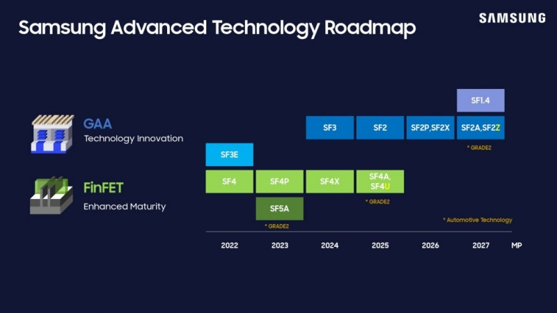
Samsung’s counterattack hinges on its GAA transistor architecture—a fundamental shift aimed at closing the technology gap. Unlike FinFET, where the gate contacts only three sides of the channel, GAA completely wraps it on all four sides, minimizing leakage and enhancing current control. This design drastically improves power efficiency and thermal management, key advantages for high-performance computing.
The shift to GAA became inevitable as transistor sizes dropped below 5nm, where FinFET structures faced current leakage and instability issues. GAA’s 360-degree control improves current efficiency by up to 30 percent and allows lower operating voltages without compromising performance. Samsung has implemented this through its Multi-Bridge-Channel FET (MBCFET) design, which stacks ultra-thin nanosheets so the gate fully envelops the channel. The result: greater scalability for AI and high-performance computing chips.
The Exynos 2600—the first chip to use Samsung’s mass-produced GAA process—has shown over sixfold improvement in neural processing unit (NPU) performance and up to 75 percent better GPU performance compared with its predecessor. Internal testing also confirmed lower heat generation and improved energy efficiency, signaling technological maturity.
Challenges remain, including the high precision and equipment complexity required for GAA production. As the process becomes more intricate, costs and initial defect rates rise. Nevertheless, industry analysts view Samsung’s GAA push as a decisive bet. Having pioneered GAA implementation at 3nm, the company is now aiming to refine the process at 2nm to achieve both higher yields and superior performance. While TSMC plans to introduce GAAFET in its own 2nm generation, Samsung’s early experience could provide a critical head start—potentially allowing it to shift the balance of power in global foundries from cost to innovation.
Similar Post