Samsung Shifts Its Technological Center of Gravity as 1c DRAM Transition Reshapes the HBM4 Landscape

Authored On
Modified
1c DRAM effectively enters the commercialization phase
Early signs of an investment-cycle recovery as demand rebounds
Samsung and SK Hynix emerge as the two-way HBM4 contenders
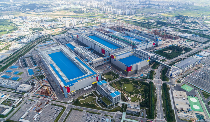
Samsung Electronics is accelerating its pivot toward advanced high-bandwidth memory (HBM) manufacturing by converting the Pyeongtaek Plant 4 into a cutting-edge HBM production line, reviving an investment cycle that had largely stalled. With yield improvements and internal incentive payouts signaling restored confidence in the technology, preparations for Plant 5 and discussions on new infrastructure suggest growing expectations of a demand rebound. Meanwhile, Micron’s redesign issues have weakened its footing in the HBM4 race, sharpening the competition between Samsung and SK Hynix to secure supply positions for Nvidia’s latest AI accelerators.
Technical validation through next-generation process migration
According to industry sources on the 13th, Samsung is set to resume cleanroom construction at its P4 line this month. Construction was halted last year but investment restarted in the third quarter, and equipment installation is now being prepared. Initially planned as a foundry-focused facility, P4 has been redesignated as a 1c DRAM production base. With power efficiency emerging as a decisive factor in HBM4 competitiveness, Samsung’s decision to convert the entire building to 1c DRAM suggests it is accelerating commercialization timelines.
The 1c node is considered the sixth generation of 10-nanometer-class DRAM, estimated at around 12–13 nm. Compared with the preceding 1b node, it narrows line widths further to improve both power efficiency and operating speed. While many viewed additional scaling beyond 1b as technologically infeasible, Samsung has sought to overcome these limits by expanding EUV usage and redesigning cell structures. Because 1c DRAM provides advantages in thickness control and stack stability—critical for HBM—it is seen as central to the company’s future competitiveness. This explains why the market considers 1c commercialization a watershed that could widen Samsung’s power-efficiency gap over rivals by several years.
The company has also recorded meaningful yield progress. Samsung’s 1c DRAM yields have recently entered the 70 percent range, considered stable for an early mass-production transition. Yields typically fall to around 50 percent when shifting from R&D lines to mass production, and about 80 percent is viewed as full-volume commercial maturity. Given that 1c development has been Samsung’s most significant challenge in regaining memory leadership, these advances suggest the company is resolving technical uncertainties ahead of HBM4. With competitors sticking to 1b for their HBM4 designs, Samsung’s move to 1c strengthens expectations that it could seize a generational advantage.
Internal recognition of progress has also been visible. Late last month, Samsung granted 4,790 treasury shares worth about 331,000 dollars to 30 engineers on the 1c DRAM development team—roughly 11,000 dollars per person—widely interpreted as a reward tied to HBM4 development milestones. In addition, Samsung recently passed Nvidia’s Product Reliability Assessment, meaning it satisfied customer requirements prior to full GPU-integration testing. Together, these developments reflect smoother-than-expected progress as Samsung works to restore confidence after difficulties with HBM3E.
A wave of factory expansion and line conversions
Amid these shifts, Samsung has begun preparing the P5 site for construction, reorganizing logistical paths and removing large volumes of steel beams previously stored onsite. The quiet but visible groundwork signals that internal approval for restarting construction has effectively been reached, contrasting sharply with the prolonged idling of the site. Even without final process blueprints, Samsung has begun executing preparatory tasks in sequential order—an indication that the company has formed a clear view on construction timelines.
Although P5 was initially expected to be built as a four-story facility, on-site planning has shifted toward a three-story structure with six cleanrooms. While this appears smaller, industry sources say the design reflects a strategy to balance phased activation with timely construction. Samsung has historically completed cleanrooms in overlapping stages across its P2–P4 projects, and a similar approach is expected here, with early and late processes integrated to maintain overall tempo.
Expectations of a revived investment cycle strengthened further after reports that Samsung will review additional Pyeongtaek infrastructure investment in the first quarter of next year. The review includes planning for large-scale utilities, civil engineering, and structural systems, interpreted as groundwork for a “mega-fab” combining DRAM, HBM, and foundry processes. The fact that Samsung is pursuing this discussion alongside ongoing equipment setups for 1b/1c DRAM and V9 NAND suggests the company sees structural demand growth as sufficiently strong to justify expanded capacity planning.
These shifts carry meaningful implications for local communities and suppliers. After years of investment delays that limited bidding opportunities, contractors now expect renewed access to P4 and P5 construction orders. Anticipated increases in labor demand also provide smaller construction and equipment suppliers with improved revenue visibility. While Samsung maintains that investments will proceed flexibly based on market conditions, the revival of activity across Pyeongtaek is widely interpreted as a sign of medium- to long-term demand recovery.
Remaining challenges: heat, speed, and yield stability
Industry attention now centers on how the HBM4 competitive landscape will take shape. With Nvidia’s next-generation AI accelerator Rubin approaching commercialization, early supply stability is expected to determine market share. Recent developments suggest a rapidly consolidating two-horse race between Samsung and SK Hynix. Micron has reportedly struggled to meet Nvidia’s required specifications and is reviewing a redesign, with internal documents suggesting the need for as much as nine additional months of development—effectively knocking it out of the early supply window.
SK Hynix has reportedly secured a supply agreement for Rubin-grade HBM4 and is awaiting final certification. Market observers believe the company is well positioned to carry forward the leadership it showed in HBM3E, supported by long-standing strengths in stack integrity, thermal management, and packaging compatibility. With capacity expansion underway at its M15X fab in Cheongju, SK Hynix is preparing aggressively for an expected surge in demand.
Samsung, meanwhile, has set supply stability and customer-trust restoration as top priorities for this generation. The company has delivered HBM4 samples to Nvidia and other customers, and internal assessments reportedly show improved metrics in thermal performance, signal speed, and stacking stability. Samsung’s unveiling of its HBM4 modules, strengthened collaboration with Nvidia, and ongoing line conversions are all viewed as significant steps. Should Samsung leverage its historical strength in high-volume manufacturing to scale HBM rapidly, analysts believe it could shift the balance of price negotiations and reshape the market.
Similar Post