Samsung flips the HBM market with HBM4 supplies to Nvidia and AMD, steps up its next-gen push

Authored On
Modified
Samsung’s HBM4 nears shipment after clearing Nvidia and AMD validation
HBM supply chain long dominated by SK hynix faces a shake-up as Samsung rebounds
Three-way race heats up among Samsung, SK hynix, and Micron as next-gen HBM battle ignites
Samsung Electronics is moving to reshape competitive dynamics in the AI chip market by pushing its sixth-generation high-bandwidth memory, HBM4. With an aggressive design strategy that significantly improved performance, Samsung has effectively locked in shipments to key customers—moving ahead of SK hynix and Micron. Having shaken off the setbacks of the fifth-generation HBM3E race, Samsung is now doubling down on next-generation product development as it seeks to secure leadership in the market ahead.
Samsung Electronics proves its presence in the HBM4 race
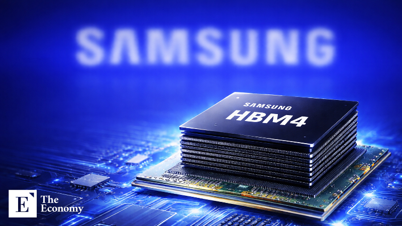
On the 25th (local time), semiconductor outlet Wccftech reported that Samsung’s HBM4 had cleared all validation tests from Nvidia and AMD, and that the company has begun preparing mass production with the goal of starting full-scale shipments next month. Late last year, Samsung was the only one—ahead of rivals Micron and SK hynix—to enter Nvidia’s final qualification test for HBM4 supply. The product is widely expected to be used in Nvidia’s next-generation AI accelerator “Vera Rubin,” slated for launch in the second half of this year, as well as AMD’s “MI450.”
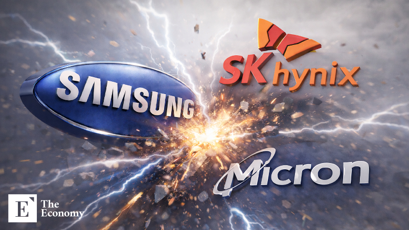
In and outside the industry, there is growing confidence that Samsung’s HBM competitiveness is entering a normalization phase. Samsung was the first in the industry to commercialize HBM2 for high-performance computing (HPC) in 2016, but it effectively withdrew from the business in 2019, citing cost burdens relative to market demand. SK hynix, by contrast, continued HBM development, became the first to commercialize HBM3, and quickly took control of the global HBM market after rising to become a key supplier to Nvidia. That first-mover advantage carried into the competition for HBM3E, its current flagship product, cementing SK hynix’s leadership.
With Samsung now securing HBM4 competitiveness, the AI semiconductor supply chain that has largely moved around SK hynix may be heading for a shake-up. The HBM market is currently defined by SK hynix’s clear lead and Micron’s pursuit, with supply struggling to keep up with demand. If Samsung—armed with overwhelming production capacity—begins to exert real influence, the supply-demand imbalance could ease and the market landscape could tilt.
What is behind Samsung’s stronger HBM4 competitiveness?
Industry observers point to an aggressive design strategy as the key driver of Samsung Electronics’ improved competitiveness. Samsung has applied its 10-nanometer-class sixth-generation (1c) DRAM process to HBM4, and is using its own foundry’s 4-nanometer process for the base die to boost time-to-delivery competitiveness—an approach that differs from SK hynix’s use of fifth-generation (1b) DRAM and a 12-nanometer logic die. With this design strategy, Samsung’s HBM4 achieved an operating speed of 11.7Gb per second, exceeding the 10Gb-per-second threshold required by Nvidia and AMD.
There may still be room for further performance gains. Samsung is said to be designing logic dies for custom HBM using processes as advanced as 2 nanometers. The company moved into 2-nanometer production in earnest after mass-producing its in-house mobile application processor, the Exynos 2600, on its first-generation 2-nanometer SF2 process in the fourth quarter of last year. An industry source said Samsung’s custom SoC team is leading the design of custom-HBM logic dies and is building a broad portfolio ranging from 4-nanometer to 2-nanometer nodes to meet diverse customer demand.
Samsung plans to apply a gate-all-around (GAA) transistor architecture to its 2-nanometer process. GAA surrounds the current-carrying channel on all four sides with a gate, increasing gate-to-channel contact area versus conventional FinFET structures, where the gate wraps three sides, and improving performance and power efficiency. Samsung, which first introduced GAA at the 3-nanometer node, is seeking further differentiation at 2 nanometers with its in-house MBCFET (multi-bridge channel FET) structure. For its part, SK hynix would need support from TSMC, its foundry partner for HBM, to keep pace—leaving it in a position where matching Samsung’s integrated capabilities would be difficult through in-house efforts alone.
HBM4E competition already under way
Having secured a meaningful foothold in the HBM4 market, Samsung Electronics is accelerating its groundwork for the next round of competition. The base die for Samsung’s next-generation custom seventh-generation HBM (HBM4E) is said to have entered the back-end design phase, marking progress beyond the midpoint of development. The back end follows front-end work such as register-transfer level (RTL) logic design and involves physical design, including placement and routing of actual circuits. Once the back end is completed, the finalized design data are handed over to the foundry for tape-out.
Samsung’s custom HBM4E base-die design is being led by members of its previous HBM development team, including a lead engineer who successfully guided the development of HBM4 based on the 10-nanometer-class sixth-generation (1c) DRAM process. After completing HBM4 development, the HBM team was reorganized under the DRAM Development Division in November last year. At the same time, Samsung is reportedly preparing to extend this work to the base-die design for custom eighth-generation HBM (HBM5). HBM design typically takes about 10 months, with the back-end stage accounting for roughly 60–70% of the process, suggesting Samsung’s custom HBM4E design could be completed around May or June this year.
Other key HBM suppliers, SK hynix and Micron, are also expected to wrap up development on a similar timeline. SK hynix has opted for a mixed-process strategy combining 12-nanometer and 3-nanometer nodes in cooperation with top foundry TSMC, while Micron is likewise leveraging TSMC processes with mass production targeted for 2027. A market expert said that as competition in the AI sector shifts from services to infrastructure buildout, leadership in the HBM4E race will hinge on which company can secure advanced memory—particularly custom HBM—capabilities first.
Similar Post