"Even Moving to Secure Equipment" Musk Launches All-Out Push for Terafab Buildout, Must Prove Competitiveness Through Yield to Overcome Skepticism

As one of the youngest members of the team, Tyler Hansbrough is a rising star in financial journalism. His fresh perspective and analytical approach bring a modern edge to business reporting. Whether he’s covering stock market trends or dissecting corporate earnings, his sharp insights resonate with the new generation of investors.
Authored On
Modified
Elon Musk Accelerates Push for ‘Computing Self-Sufficiency’ via Terafab Project
Formalizes Cooperation with Intel While Engaging Semiconductor Equipment Makers
Semiconductor Competitiveness Hinges on Yield, Can It Reverse Market Sentiment
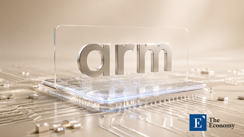
Elon Musk, CEO of Tesla, is accelerating the development of the ‘Terafab’ project. Following the formalization of cooperation with Intel Foundry earlier this month, Musk has moved to engage leading semiconductor equipment manufacturers in rapid succession, stepping up efforts to construct an in-house semiconductor production base. However, skepticism surrounding Musk’s vision remains firmly entrenched in the market, with analysts indicating that securing meaningful yield levels will be essential to overturn such sentiment.
Terafab Construction Blueprint
On April 16 (local time), Bloomberg reported that Musk’s Terafab team has contacted the world’s three largest semiconductor equipment makers—Applied Materials (AMAT), Tokyo Electron (TEL), and Lam Research—to inquire about equipment pricing and delivery timelines. The team reportedly issued bulk requests for quotes covering the full semiconductor production process, including photomasks, substrates, etchers, deposition systems, and cleaning equipment. It is also said to have offered to pay significantly above quoted prices in exchange for priority supply.
The Terafab team additionally sought support from Samsung Electronics, its semiconductor production partner, though Samsung is reported to have counterproposed expanding production capacity at Tesla’s foundry facility currently under construction in Taylor, Texas.
Musk is also intensifying hiring efforts to staff the Terafab project. Tesla recently posted job openings for Terafab engineers, offering substantial compensation packages. For instance, semiconductor system-on-chip (SoC) development engineers are offered annual salaries ranging from $88,000 to $248,000, along with additional stock-based compensation. This has reignited already fierce global competition for semiconductor talent.
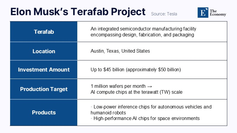
Terafab is a comprehensive semiconductor hub being built by Musk in Austin, Texas, designed as a vertically integrated facility encompassing design, manufacturing, and testing. The site is expected to produce low-power inference chips for Tesla’s autonomous vehicles and humanoid robot ‘Optimus,’ as well as high-performance AI chips capable of operating in space environments. Musk’s stated goal is to secure annual computing capacity of 1 terawatt (TW) through Terafab. Bernstein and other major investment banks estimate that realizing this vision would require an astronomical capital investment ranging from at least $5 trillion to as much as $13 trillion.
Widespread Market Skepticism
Market skepticism toward the Terafab project continues to intensify. Critics argue that the scale of the project is excessively large for a company with no prior experience in advanced foundry operations. Tesla has historically outsourced chip production to external foundries such as Samsung Electronics, and Musk’s target of 1 terawatt in computing capacity is nearly 50 times the global annual computing power output, which stands at approximately 20 gigawatts (GW).
Concerns are further amplified by uncertainty surrounding the procurement of extreme ultraviolet (EUV) lithography equipment, exclusively supplied by ASML in the Netherlands. Critics contend that advancing mass production plans without securing such critical equipment is unrealistic.
Musk, however, has firmly rejected these pessimistic views. In a post on social media platform X (formerly Twitter) last month, he stated, “While many companies have succeeded in chip production, not a single one has built fully reusable rockets or achieved the scale of SpaceX.” While acknowledging the extreme complexity of semiconductor manufacturing, Musk argued that such challenges do not constitute an “impossible endeavor” for a company that has led advancements in rocket science through SpaceX. He also emphasized that the project has been designed with two separate fabs, each dedicated to producing a single chip, asserting that this simplified structure would be more efficient and easier to control than conventional foundry models.
Several companies have begun aligning with Musk’s vision. Intel is a prominent example. On April 7, Intel announced via its official X account that it would participate in the Terafab project alongside SpaceX, xAI, and Tesla to help redefine silicon fab technology. Intel’s involvement is expected to center on providing its 18A (1.8nm) process technology. Industry observers note that while the project could present an opportunity for Intel’s foundry business revival, its current 18A process yield—reportedly around 60%—suggests that near-term execution may prove challenging.
Yield Barrier to Determine Market Position
Musk’s aggressive push into in-house semiconductor production reflects a broader strategy to secure computing power in the AI era. Tesla’s autonomous driving and robotics operations, xAI’s model development, and SpaceX’s space infrastructure all require vast quantities of chips. Should the Terafab project succeed, Musk would effectively internalize the computing supply chain across his industrial ecosystem, gaining direct control over AI infrastructure and computing power while strengthening his position in advanced industries.
The critical question going forward is whether Terafab can achieve yield levels acceptable to the market. Yield refers to the proportion of functional chips produced from a wafer and serves as a key indicator of manufacturing efficiency. It is widely regarded as a decisive factor influencing product success and market positioning, particularly in the early stages of production. High yield enables more usable chips at the same cost, improving both cost competitiveness and profitability. Conversely, low yield constrains effective output despite increased production and can significantly amplify losses, especially in advanced process nodes.
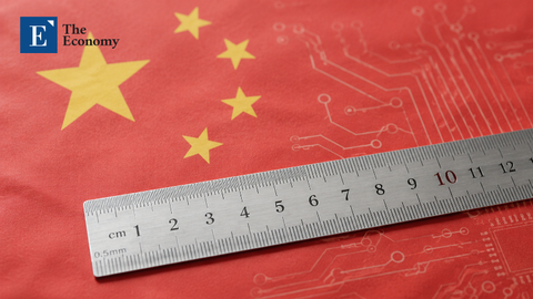
Numerous companies have struggled to compete due to yield challenges. A representative case is SMIC (Semiconductor Manufacturing International Corp.), China’s largest foundry. Its 5nm process yield is reportedly only around 20%. U.S. export restrictions have blocked access to EUV lithography equipment supplied exclusively by ASML, delaying progress in advanced process development. The market generally views it as difficult for SMIC to compete in the near term with TSMC and Samsung Electronics, which have achieved relatively stable yields in leading-edge nodes such as 2nm.
As one of the youngest members of the team, Tyler Hansbrough is a rising star in financial journalism. His fresh perspective and analytical approach bring a modern edge to business reporting. Whether he’s covering stock market trends or dissecting corporate earnings, his sharp insights resonate with the new generation of investors.
Similar Post