K-Semiconductors Reject Japan’s ‘Half-Price Fab’ Over Security Concerns

Authored On
Modified
Technological Security and National Asset Protection as Top Priorities
Japan Accelerates All-Out Efforts for Semiconductor Revival
Clear Practical Constraints Despite Subsidy Inducements
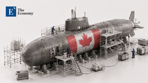
The Japanese government proposed a comprehensive package including subsidies, tax incentives, and infrastructure to Samsung Electronics and SK hynix for the establishment of domestic production lines. However, reports indicate that the 두 companies declined the offer, citing concerns over technology leakage and the protection of the domestic semiconductor ecosystem.
Amidst intensified global semiconductor subsidy competition, while firms like Taiwan’s TSMC have settled in Japan, Korean companies concentrate on maintaining their unique technological gap by strengthening investment plans in domestic hubs, including the Yongin Cluster. Market attention focuses on the strategic move of K-semiconductor, which prioritizes technological security in an era of astronomical costs.
Security Risks and Strategic Tech Control
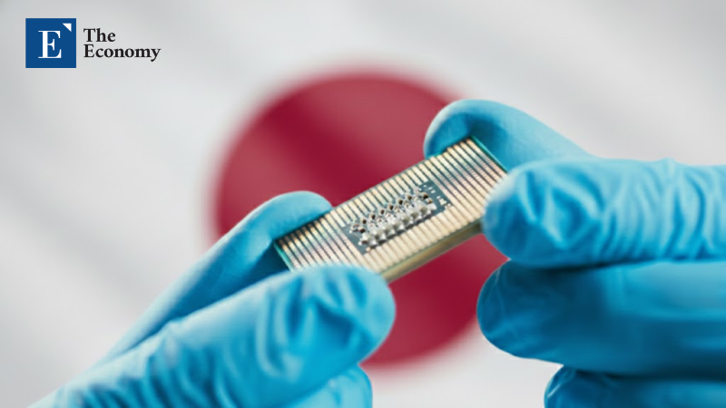
According to the IT specialized media Wccftech, the Japanese administration repeatedly offered astronomical subsidies and logistics infrastructure packages to Korean companies to complete its domestic semiconductor supply chain. However, Samsung Electronics and SK hynix rejected all such proposals for factory construction in Japan, prioritizing concerns about technology leakage and the protection of the domestic semiconductor ecosystem. Previously, Nihon Keizai Shimbun reported on the 21st that “SK hynix is considering building a memory fab in Japan,” but SK hynix immediately denied this.
Japan’s incentive lies in providing free sites and infrastructure such as power and water to reduce the Total Cost of Ownership (TCO) by up to 50% compared to Korea. Considering the reality that constructing a single advanced semiconductor fab typically costs approximately $13.89 billion, such an offer represents an overwhelming incentive equivalent to receiving billions of dollars in cash for corporate management. A senior official from Samsung Electronics’ semiconductor division also admitted, “In terms of TCO, including investment costs, the cost of building and operating a memory production line in Japan is half the level of that in Korea.”
Nevertheless, Samsung Electronics and SK hynix chose to remain in Korea, prioritizing technological security. This decision stems from the judgment that since advanced memory processes are classified as national core technologies, establishing overseas production facilities poses a high risk of becoming a channel for unintended technology transfer or the leakage of core personnel. An industry official explained, “It is true that both companies face domestic risks that hinder concentration on core business, such as cost leakage and pressure for decentralized investment depending on the administration, but they push ahead with the creation of domestic clusters to maintain their unique technological superiority and secure control over national security.”
In fact, Samsung Electronics and SK hynix practice their commitment to concentrated domestic investment by carrying out large-scale projects, investing $250 billion and $416.67 billion respectively in the Yongin System Semiconductor Cluster by 2042. This vividly reveals the nature of the memory semiconductor industry, where manufacturing efficiency and security are absolute values, and suggests that safeguarding long-term technological sovereignty and stabilizing the domestic manufacturing ecosystem are the top priorities. While Japan’s support measures may provide temporary benefits, they carry the possibility of becoming a boomerang in the form of shrinking domestic employment and the transfer of industrial leadership overseas.
Japan’s State-Led Semiconductor Reconstruction Strategy
The global semiconductor market shifted toward a competition for supply chain reorganization led by massive subsidies since the former Biden administration in the U.S. enacted the CHIPS Act in 2022, announcing a plan to provide $52.7 billion over five years. Policy competition to secure domestic production bases began in earnest, and major companies including Samsung Electronics and SK hynix engaged in local investments in the U.S. China announced a plan to invest approximately $84.6 billion, and the EU also embarked on attracting companies through the $42.6 billion ‘EU Chips Act.’ National finances established themselves as a core tool of semiconductor industrial strategy.
Japan took aggressive financial measures under the same stance. The Japanese government decided to provide a total of $7.74 billion in subsidies to Taiwan’s TSMC for building factories in Japan. The structure involves supporting $3.07 billion for the first plant and $4.71 billion for the second plant out of a total of $19.1 billion invested in the two plants of JASM, TSMC’s Japanese subsidiary established in Kumamoto Prefecture. The JASM 1st plant, which began operation in December 2024, is mass-producing 12-28nm logic semiconductors, while the 2nd plant aims for 6nm-class production with a planned start in 2027. This serves as a turning point for Japan to raise its technological level, which remained at the 40nm class.
Recently, support for the state-backed semiconductor company Rapidus expanded further. The Ministry of Economy, Trade and Industry (METI) of Japan announced an additional support of up to $6.45 billion for Rapidus’ 2026-2027 projects, including a direct government investment of $645.16 million through the Information-technology Promotion Agency (IPA). Accordingly, cumulative government support for Rapidus is expected to reach $18.71 billion by 2027. A characteristic of the policy shift is that the system allows the state to directly secure stakes in private technology companies instead of the previous simple subsidy method.
Rapidus prepares for the operation of the Hokkaido Chitose IIM-1 plant with the goal of mass-producing 2nm logic semiconductors in 2027. To this end, it installed more than 200 units of advanced equipment, including ASML’s mass-production Extreme Ultraviolet (EUV) lithography equipment, last December. The plan shortens the 2nm manufacturing lead time from the previous 120-day level to 50 days, ensuring that urgent lots finish production within 15 days. Considering that the Japanese government set a goal of investing $64.52 billion in the AI and semiconductor sectors by 2030 to raise the total sales of the production industry to more than $96.77 billion, Japan’s semiconductor strategy expands into a state-led industrial reconstruction model built upon subsidy policies.
Complex Calculus of Cost and Efficiency Amid ‘Super Cycle’
As the scale of funds required for semiconductor factory construction expanded incomparably with the past, the massive subsidies and cost reduction packages presented by various governments act as substantial investment variables for companies. Until the 2010s, the construction cost for advanced fabs was mentioned at around $6.94 billion per unit, but recently it soared to more than $13.89 billion, and some observations suggest that $83.33 billion is needed for the entire factory construction. For example, it is estimated that more than $41.67 billion will be invested in Pyeongtaek Campus Line 5, which Samsung Electronics pursues, a fourfold increase compared to the $10.83 billion invested in Pyeongtaek Line 1 completed in 2014.
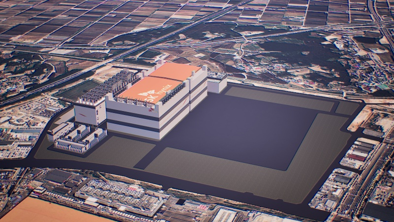
SK hynix also already invested $13.89 billion in building the Cheongju M15X fab, and the Yongin 1st fab, scheduled for completion in the first half of 2027, is expected to be larger than this. Regarding the overall plan for the Yongin Semiconductor General Industrial Complex, a total of $83.33 billion was initially expected in 2019, but now that forecasts suggest more than $83.33 billion is needed per factory, the total investment scale jumped to $416.67 billion. Securing large sites, upward adjustment of the floor area ratio, factory designs expanded from 2 floors to 3 floors, and the expansion of clean rooms act as cost-increasing factors. Added to this is a structure in which total investment costs continue to expand, such as expanding cooling facilities due to increased power usage, establishing high-level clean systems, and introducing renewable energy and water recycling facilities.
However, even in this situation, Samsung Electronics and SK hynix appear to focus more on the values of technological security and operational efficiency. This reflects the calculation that since the memory industry recently entered the so-called ‘super cycle’ and profitability improved, the factors to be considered for relocating production bases solely for cost reduction remain very complex. The memory industry is sensitive to economic fluctuations, and there is a possibility that large-scale expansion lead to oversupply; for this reason, expanding overseas production is perceived as an issue involving both technological management and policy risks. For companies, market outlook, technology protection, and investment continuity carry more weight than the scale of subsidies.
Similar Post