Glass Substrates Tackling AI’s Biggest Heat Challenge Become Flashpoint in Global Race for Technological Dominance

Authored On
Modified
Chips Are Growing Hotter and Larger: “Plastic Can No Longer Withstand It”
Glass Substrates Emerge as the ‘Universal Fix’ for AI’s Biggest Heat Challenge
Thinner Packaging Possible Without an Intermediate Interposer
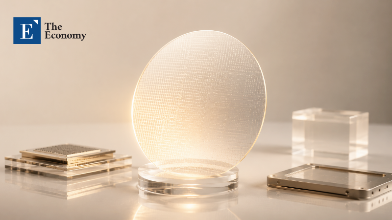
Competition among domestic and overseas companies is intensifying over the commercialization of glass substrates, now drawing attention as a core technology in next-generation semiconductor packaging. As demand for high-performance artificial intelligence (AI) chips surges, the physical limits of existing substrates (FC-BGA) have come into sharper focus, elevating glass substrates—advantageous in thermal stability and fine-circuit implementation—as a key alternative. Market attention is also shifting from technology competition to the timing of mass production and the potential for monetization.
Nvidia Forms ‘Glass Alliance’ With Corning
On the 6th, local time, Nvidia and Corning, the U.S.-based glass and optical fiber manufacturer, announced that they had signed a multiyear commercial and technology partnership to supply optical connectivity solutions required for next-generation AI infrastructure. Under the agreement, Corning plans to expand its U.S. optical connectivity production capacity tenfold and increase optical fiber output by 50%. To that end, it will build three advanced manufacturing facilities in North Carolina and Texas and create roughly 3,000 new jobs. Through the partnership, Nvidia secured the right to invest up to $3.2 billion in Corning. Nvidia also obtained warrants to purchase 15 million Corning shares at $180 per share and separately made an advance payment of $500 million.
The core of the partnership is the “exit of copper.” Industry observers believe Nvidia has begun to fully recognize the limits of existing copper-wire-based connectivity structures in the process of upgrading AI data centers. The rapid expansion of AI computing workloads has heightened the need to improve data transmission speeds and power efficiency. Existing data centers exchanged electrical signals through copper wiring. But as AI models grew larger and data transmission volumes surged, copper wires ran into physical constraints in the form of heat generation and resistance.
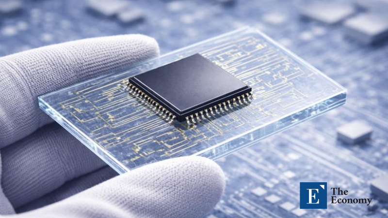
By contrast, optical transmission systems using glass substrates and optical fiber are assessed to deliver faster data transfer speeds than conventional copper wires while consuming five to 20 times less power. In particular, glass substrates significantly outperform existing plastic-based substrates in thermal stability, surface flatness and transmission characteristics, enabling them to help resolve bottlenecks in high-performance chip packaging. This is a key lever for simultaneously reducing power burdens and heat issues in AI data centers. Nvidia Chief Executive Officer Jensen Huang designated the technology at GTC 2025 last year as an essential element for scaling AI infrastructure. Nvidia plans to fully introduce co-packaged optics (CPO), a technology that brings Corning’s optical fiber close to the chip, into its next-generation systems.
Commercialization Race From Intel to Apple
Investment in glass substrates by global Big Tech companies has already been underway for several years. Intel is a frontrunner in glass substrates and has conducted research and development (R&D) for more than a decade. Since last year, it has been exploring patent licensing with multiple semiconductor glass substrate manufacturers and materials, components and equipment suppliers. The model allows patents to be used under certain periods and conditions in exchange for royalties. Last month, Intel also invested more than $1 billion in its Chandler, Arizona facility to build R&D and pilot infrastructure. The core of Intel’s technology lies in combining its proprietary advanced packaging solution, Embedded Multi-die Interconnect Bridge (EMIB), with next-generation substrate technology. EMIB is an interconnect technology that links different chips at high speed and has already demonstrated performance scalability through application in some high-performance products.
AMD has established a technology roadmap for pilot production of semiconductor glass substrates in 2026 and product application in 2028. This marks the first confirmed glass substrate roadmap in the semiconductor industry, with AMD planning to first apply glass substrates to semiconductor chip interposers. Interposers are used in packaging AI accelerators and serve as the connection pathway between a centrally located graphics processing unit (GPU) and high-bandwidth memory (HBM) positioned around it. Current interposers use silicon, which is costly and presents numerous process challenges, including warpage. Glass substrates have less warpage than silicon. They are also easier to planarize and can support finer circuit implementation.
Tesla and Apple are also known to have reviewed the technology through meetings with glass substrate manufacturers. At those meetings, they were briefed on semiconductor glass substrate technology and explored potential cooperation. Market observers expect Apple to use glass substrates in servers and data centers that form part of its AI infrastructure. Tesla is said to be reviewing glass substrates to complete the architecture of full self-driving (FSD) chips and infotainment chips that can operate stably even under high temperatures.
Broadcom, regarded as a potential second Nvidia, is also conducting performance evaluations to apply glass substrates to semiconductor chips. Broadcom’s move is drawing attention because it signals the expansion of the glass substrate market. Broadcom is an ASIC semiconductor company that designs and manufactures chips tailored to customer orders for specific applications. According to JPMorgan, Broadcom holds a 55% to 60% share of the global market, meaning its full-scale adoption could rapidly spread glass substrates across the semiconductor industry. Commercialization of glass substrates is expected after 2027. Market research firm MarketsandMarkets forecasts the global glass substrate market will grow to $8.4 billion by 2028.
Samsung, SK and LG Move to Seize Glass Substrate Leadership
Domestic companies are also moving aggressively to secure an early position in glass substrates. In Korea, Samsung Electro-Mechanics, SKC and LG Innotek are currently working toward glass substrate commercialization. Samsung Electro-Mechanics is accelerating both technology competition and customer acquisition strategy. According to industry sources, Samsung Electro-Mechanics recently supplied glass substrate samples to Apple following Broadcom, entering the validation pipeline of global Big Tech companies. It is producing prototypes through a pilot line established at its Sejong plant and is targeting mass production after 2027 following pilot production this year. While Intel has emphasized technology direction and ecosystem building, Samsung Electro-Mechanics is seen as pursuing a strategy of first securing commercialization results by preempting contact points with key customers such as Apple.
SKC is preparing for mass production through its subsidiary Absolics, which has built a plant in Covington, Georgia. Absolics is considered one of the fastest movers in terms of production infrastructure. SKC plans to invest about 60% of the funds secured through its recent paid-in capital increase, or roughly $408 million, into Absolics’ product development and process stabilization. However, it still faces the tasks of securing certification from global customers and achieving economically viable yields, and the pace of commercialization appears to have become somewhat more cautious than market expectations. Even with facilities in place first, actual competitiveness is expected to be determined by process maturity and yield levels.
LG Innotek is continuing a strategy of strengthening fundamentals while monitoring market demand. LG Innotek has established a glass substrate sample production system at its Gumi plant and aims for commercialization in 2030. In January, it also partnered with precision glass processing company UTI to strengthen core technologies while building a pilot production line at a domestic site for development. President Moon Hyuk-soo’s remarks that the company’s mass-production target is 2028, while full-fledged market demand may emerge around 2030, are interpreted as a strategy to align technology maturity and market timing rather than pursue an excessive speed race.
Domestic component companies are also joining the supply chain and accelerating glass substrate development. JWMT, in which Samsung Electronics has invested, possesses through-glass via (TGV) technology. TGV is a core process that creates data pathways by drilling vertical holes through glass substrates. JWMT has advanced technology for drilling microscopic holes into fragile glass. Extol has also received investment from Samsung Electro-Mechanics and is advancing plating technology required for glass substrates. Unlike plastic, glass has a smooth surface, making plating difficult, but Extol possesses technology that fills TGV-drilled pathways with copper to allow electrical signals to flow.
The key to glass substrates is raising yield. Because glass is fragile, the risk of damage is high during transportation or processing. In particular, TGV, which requires tens of thousands of microscopic holes to be drilled into a substrate, causes yield to fall if even one issue arises in hole position, size, shape or glass damage. One semiconductor industry official said, “The success or failure of mass-producing glass substrates depends on how effectively defect rates are controlled in this demanding TGV process,” adding, “It is essential to build a close cooperative ecosystem with materials, components and equipment companies that handle specialized equipment and related technologies.”
- Previous “Countdown to a Bilateral Military Alliance” India and Russia Open Military Bases to Each Other, Building an ‘Energy-Security Complex’ to Contain China’s Expansion
- Next China Erasure Gains Momentum Across Europe as EU Moves to Block Chinese Industrial Offensive, Beijing Prepares Retaliation
Similar Post