Glass Substrates Emerge as AI Semiconductor Game Changer as Mass Production Race Intensifies at Home and Abroad; Overcoming Glass Brittleness Seen as Key Hurdle

Authored On
Modified
Glass Substrates Gain Traction in AI Era as Next-Generation Packaging Alternative
SKC, Samsung Electro-Mechanics, LG Innotek Accelerate Production Line Build-Out and Prototype Development
U.S., Japan, China Join Fray in Escalating Competition to Establish Mass Production Framework
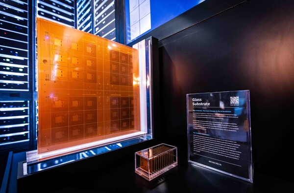
Competition among domestic and global companies is intensifying over the commercialization of glass core substrates, which are drawing attention as a pivotal technology in next-generation semiconductor packaging. Glass substrates are emerging as an alternative capable of alleviating bottlenecks in the packaging stage that determine the performance of artificial intelligence (AI) semiconductors. In response, Korean companies including SK, Samsung, and LG, along with major semiconductor powerhouses such as the United States, Taiwan, and Japan, are expanding related investment and research efforts to secure early market leadership. With Chinese firms recently joining the technology race, industry observers expect that future dominance in the glass substrate market will hinge not only on technological sophistication but also on mass production capabilities and supply chain establishment.
Acceleration of Development Race Among SK, Samsung, and LG
According to the investment banking (IB) industry on the 27th, SKC convened its board of directors the previous day and approved a capital increase worth approximately $690 million to reinforce its glass substrate business. Of the funds to be raised, roughly 60%, equivalent to about $407 million, will be allocated to product development at Absolics, its glass substrate subsidiary. Having identified glass substrates as a future growth engine, SKC has provided sustained backing since acquiring Absolics, including four separate payment guarantees.
Absolics plans to pursue a dual-track strategy aimed at timely market entry by simultaneously developing an “Embedding” approach for high-end AI data center applications and a faster-to-commercialize “Non-Embedding” model. SKC stated that Absolics has recently achieved meaningful progress in product development for global Big Tech clients and is consolidating specialized engineering expertise under newly appointed CEO Jiho Kang, formerly of Intel and SK hynix.
Samsung Electro-Mechanics is also accelerating its push. After formally declaring its market entry in early 2024, the company established a pilot glass substrate line at its Sejong facility in June last year and commenced production. In November of the same year, it delivered its first samples to a global Big Tech client. In December, it signed a memorandum of understanding (MOU) with Japan’s Sumitomo Chemical Group to review the establishment of a joint venture related to glass substrate material manufacturing.
LG Innotek is likewise building a pilot production line for glass substrates at its Gumi plant. The company manufactured prototypes at the end of last year and aims to commence mass production between 2027 and 2028. LG Innotek intends to enhance its business competitiveness by applying glass substrate technology to its flagship high-value semiconductor substrate product, FC-BGA (Flip-chip Ball Grid Array). To that end, it is actively collaborating with global clients and domestic and overseas companies possessing relevant glass substrate technologies to accelerate development.
Intel, TSMC, and Intensifying Chinese Pursuit
Global players are also moving swiftly. Intel unveiled a thick-core glass substrate integrating EMIB (Embedded Multi-die Interconnect Bridge) at “NEPCON JAPAN 2026,” held at Tokyo Big Sight from the 21st to the 23rd of last month. The glass substrate presented by Intel is designed for a 78×77mm package and supports a silicon area of approximately 1,716mm² (2×858mm²) to enable large-scale configurations beyond reticle limits. The company introduced a so-called 10-2-10 thick glass core structure, featuring 10 redistribution layers (RDL) on both the upper and lower sides, enabling fine-pitch routing on the top while facilitating mainboard/PCB connectivity on the bottom.
Visionox, one of China’s three largest display manufacturers, has also begun large-scale investment in the glass substrate business this year. The company initiated efforts to build a supply chain encompassing materials, components, and equipment in the second half of last year and is currently engaged in technology development discussions with Korean suppliers. An industry official noted that Visionox is positioning semiconductor glass substrates as a new growth driver and is moving to secure the technologies necessary for market entry.
China’s largest display maker, BOE Technology, is likewise concentrating on the glass substrate business. BOE completed technical verification and feasibility reviews for mass production last year and has launched the business. In addition, Chinese printed circuit board (PCB) manufacturer AKM Meadville has established a pilot production line, while outsourced semiconductor assembly and test (OSAT) firm Yuntian Semiconductor has already been incorporated into Huawei’s supply chain, gaining recognition for its glass substrate technology. Taiwan’s TSMC and Japan’s Rapidus have also entered the glass substrate arena. Most companies have set mass production targets between 2027 and 2030, placing heightened attention on which player will first achieve commercial-scale output.
Rising Chip Heat and Scale Render Plastic Substrates Unsustainable
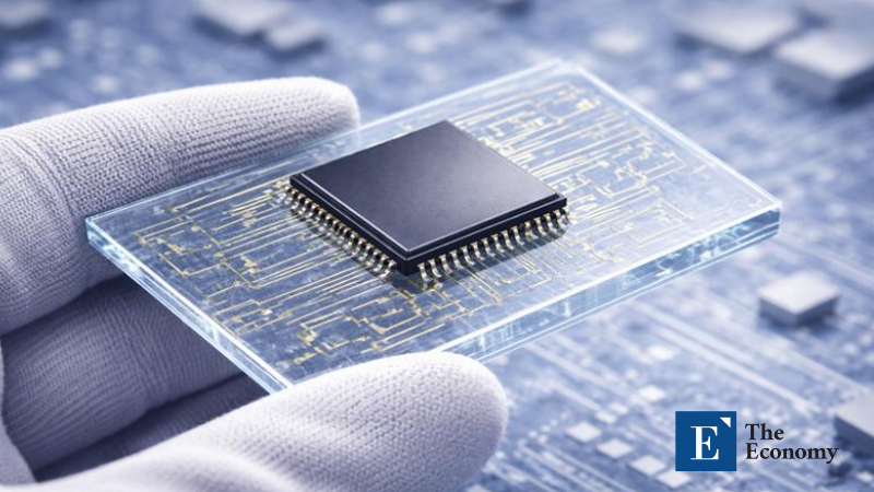
The growing importance of glass substrates stems from their ability to overcome the fundamental limitations of conventional carbon-based plastic (organic) substrates. Semiconductor substrates serve as structural platforms that connect semiconductor chips to mainboards, transmitting electrical signals and providing protection against external impact. While organic substrates are currently predominant, their critical limitations have become increasingly apparent amid circuit miniaturization and the rising use of high-performance semiconductors such as multi-chip packages (MCP).
Signal attenuation and error frequency increase during data transmission. Heat generated during GPU operation can physically deform substrates and weaken interconnections between semiconductors. Moreover, leading-edge chips now rely on ultra-fine interconnects with widths below 2 micrometers, which are difficult to etch onto organic substrates. Substantial power loss during electricity delivery further compounds the issue, with AI operations consuming several hundred watts of power. Silicon substrates are widely used as an alternative, yet they face constraints in scalability and entail high manufacturing costs.
By contrast, glass substrates offer thin profiles and smooth surfaces conducive to fine circuit implementation, along with superior resistance to heat and warpage. They enable a reduction in intermediary substrates, allowing overall substrate thickness to be decreased by up to 25% and power consumption to be reduced by approximately 30%. Their capacity to maximize AI semiconductor integration density also enhances AI server and GPU performance thresholds. In addition, glass substrates can directly connect semiconductor chips to mainboards without silicon interposers, paving the way for cost reduction and package miniaturization.
Industry outlooks remain positive. AMD is reportedly reviewing the application of glass substrates to high-performance computing (HPC) semiconductors by 2028, while Broadcom, Nvidia, and Tesla are also evaluating potential adoption. Market growth prospects are likewise evident. According to global market research firm TBRC, the glass substrate market is projected to expand at a compound annual growth rate of 6.6%, growing from $7.9 billion last year to approximately $10.85 billion by 2029. Although the market remains relatively small at present, analysts assess that it is entering a sustained growth phase alongside the expansion of AI and HPC.
Nevertheless, concerns persist regarding the completeness of early commercial products. Even if glass substrates are introduced in the near term, first-generation offerings may resemble beta-stage products with limited maturity. Industry sources also cite brittleness as the most pressing technical challenge. As glass substrates become thinner, susceptibility to micro-defects increases, leading to fracture or delamination phenomena such as SeWaRe. Reliability issues therefore remain a critical obstacle to full-scale commercialization.
Similar Post