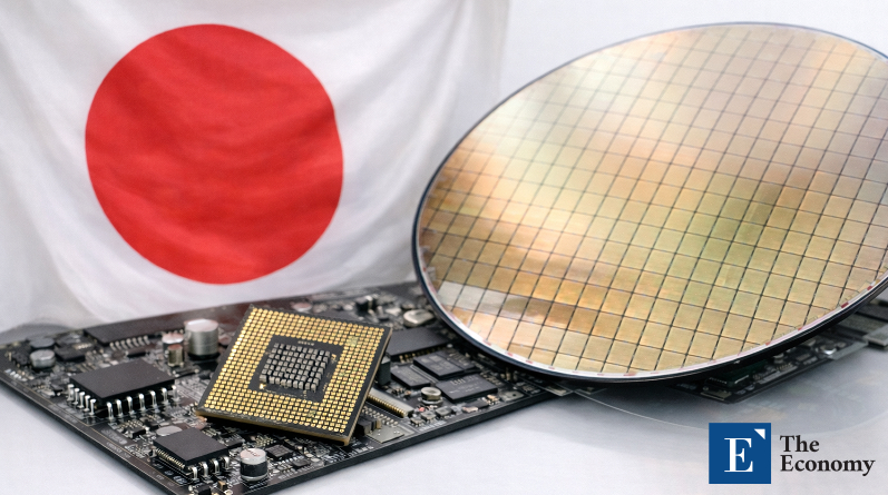
Japan Accelerates Semiconductor Revival with Aggressive Investments in Foundries and Materials, Components and Equipment

Authored On
Modified
Japan Mounts All-Out Push for Semiconductor Self-Reliance Through R&D Hub Development
Will Japan’s Materials, Components and Equipment Sector, a Pillar of the Global Supply Chain, Further Expand Its Market Dominance?
Massive Capital Injections Flow to Foundries Including TSMC and Rapidus
The Japanese government is intensifying efforts to establish a self-sustaining domestic semiconductor ecosystem. It is deploying substantial capital into foundries, a central axis of advanced chip competition, while simultaneously building research and development (R&D) hubs to bolster the growth of local materials, components and equipment suppliers. Should these firms—already wielding formidable influence in global markets—achieve further expansion, Japan’s semiconductor value chain competitiveness is expected to strengthen markedly.
Government-Backed Advanced Equipment R&D Hubs
According to Nikkei Asia on Feb. 26, Japan’s Ministry of Economy, Trade and Industry plans to establish semiconductor R&D hubs equipped with high-cost design software and state-of-the-art equipment, making them accessible to companies and universities at affordable rates. The government will invest approximately $870 million to construct three specialized core facilities tailored by function. The initiative is widely interpreted as a strategy to cultivate a robust upstream industrial base capable of supplying advanced equipment and materials to foundries such as TSMC, which has established production facilities in Japan, and Rapidus, a government-backed venture.
The Tokyo design hub, slated for completion this fall, will house automated design tools (EDA) worth tens of millions of dollars, along with computing servers and technical specialists, lowering entry barriers for small and mid-sized fabless firms. The Chitose equipment and materials hub, scheduled for completion in 2029 near Rapidus’ Hokkaido plant, will secure ASML’s latest extreme ultraviolet (EUV) lithography systems to support prototype testing for domestic equipment and materials companies. A compound semiconductor testing center will focus on next-generation materials such as gallium nitride (GaN), targeting advanced industries including artificial intelligence data centers, electric vehicles and 6G communications.
Nikkei noted that “the more cutting-edge the semiconductor field becomes, the more costly R&D grows, making it difficult for companies to invest independently,” adding that “design support software and next-generation lithography systems can cost hundreds of millions of dollars per unit, requiring government support to lay the foundation for private-sector technology development.” The hub initiative ultimately aims to reinforce the industrial underpinnings of Japan’s semiconductor sector and solidify its domestic value chain through infrastructure support.
Global Competitiveness of Japan’s Materials, Components and Equipment Firms
The government’s blueprint is expected to create additional growth opportunities for Japan’s materials, components and equipment companies, which underpin the global semiconductor supply chain. Japan already possesses a substantial roster of globally competitive suppliers. Ajinomoto Group, widely known for its MSG products, commands more than 90% of the semiconductor packaging insulation film market through its Ajinomoto Build-up Film (ABF). Produced by its precision chemicals subsidiary Ajinomoto Fine-Techno, ABF serves as an insulating film used in substrates for high-performance central processing units (CPUs) and graphics processing units (GPUs), playing a critical buffering role within chip dies.
Nittobo, a leader in the textile industry, is effectively the world’s sole supplier of T-glass. This ultra-fine glass fiber cloth, characterized by an exceptionally low coefficient of thermal expansion (CTE), is used as a reinforcing material in semiconductor substrates to mitigate warpage during advanced chip packaging processes. Lasertec, which operates in semiconductor inspection and measurement equipment, is the only company globally to supply photomask inspection systems for EUV lithography.
JSR is a world-class manufacturer of photoresist chemicals, indispensable photosensitive materials for advanced photolithography. These materials are coated onto silicon wafers before EUV lithography systems etch intricate circuit patterns. Tokyo Electron, a key semiconductor equipment manufacturer, also stands out in EUV photoresist coating and development systems. The Semiconductor Equipment and Materials International (SEMI) association assessed that “when integrated with lithography systems, Tokyo Electron’s equipment forms an indispensable chain that accounts for virtually the entire market share in coating and cleaning systems for advanced lithography technologies.”
In addition, Sumco and Shin-Etsu Chemical in silicon wafer manufacturing; Disco in wafer dicing; Advantest in automated test equipment (ATE); Daifuku in cleanroom transport solutions; Ebara in chemical mechanical polishing (CMP); Screen Holdings in wafer cleaning systems; Kokusai Electric in deposition equipment for semiconductor fabrication facilities; and Hamamatsu Photonics in optical sensors and measurement devices for wafer inspection all play critical roles in the global semiconductor supply chain. With government-backed infrastructure support, further growth by these companies would significantly elevate Japan’s semiconductor ecosystem competitiveness.

Blazing Pace of Public-Private Capital Deployment
Japan’s support extends beyond materials and equipment to foundry operators. Between 2021 and 2024, the government implemented semiconductor and AI support strategies totaling approximately $27 billion, equivalent to nearly 0.7% of gross domestic product. This level of support surpasses the scale of the U.S. Chips and Science Act, which amounts to roughly 0.2% of GDP. A primary beneficiary has been TSMC, which began operations at its Kumamoto plant in 2024. The company received $8 billion in subsidies from the Japanese government for the facility, which produces 12–28 nanometer chips for automotive and consumer electronics applications and is pursuing construction of a second plant aimed at introducing a 3 nanometer-class advanced process.
In November last year, the government unveiled an additional $67 billion subsidy package centered on three pillars: attracting overseas factories, nurturing domestic champions and strengthening equipment industry competitiveness. The “domestic champion” designation is widely understood to refer to Rapidus. Established in 2022 to spearhead Japan’s semiconductor resurgence, Rapidus has expanded its capabilities with government backing. The Ministry of Economy, Trade and Industry plans to inject an additional $6.7 billion into Rapidus during fiscal years 2026–2027, bringing total state support to approximately $19 billion.
Private-sector commitment is equally pronounced. Thirty leading Japanese corporations plan to collectively invest about $1.1 billion in Rapidus in the near term. SoftBank established SAIMEMORY in late 2024 to pursue memory semiconductor R&D as well as manufacturing and sales operations, launching full-scale operations in July last year. SoftBank plans to invest a total of $21 million in SAIMEMORY by 2027, while Japan’s national research institute RIKEN and Fujitsu, also participating in SAIMEMORY, are reportedly reviewing investments of approximately $6.7 million each.
Similar Post