“From TSMC to Samsung, Intel and Rapidus,” the 1-Nanometer Race Heats Up as Tesla Turns to In-House Production to Mitigate Risk

Authored On
Modified
TSMC, poised to begin mass production of 1.6-nanometer chips, is also moving in earnest to develop a 1.4-nanometer process
Rapidus, Intel and Samsung Electronics are likewise drawing up plans for mass production in the 1-nanometer range
Elon Musk is pushing to build his own semiconductor plant and diversify supply chains

Competition in the semiconductor industry over the 1-nanometer (nm, one-billionth of a meter) process is beginning in earnest. Major foundry players including TSMC, Samsung Electronics, Rapidus and Intel have started presenting back-to-back roadmaps for 1-nanometer mass production as they step up efforts to secure an early lead in the market. Against that backdrop, some companies, including Tesla led by Chief Executive Officer Elon Musk, are also accelerating efforts to build their own supply chains in order to minimize uncertainty amid the fierce race for leading-edge chips.
TSMC’s 1-Nanometer Roadmap
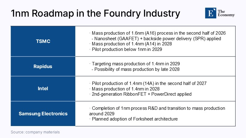
On April 20, Taiwanese media outlets including China Times, citing sources, reported that reservations for TSMC’s 2-nanometer (N2P) products had already been filled through 2028 production and that mass production is scheduled to begin in the fourth quarter of this year. The sources added that TSMC plans to mass-produce its cutting-edge A14 (1.4-nanometer) process chips in 2028 and begin trial production of sub-1-nanometer chips in 2029. TSMC’s 1.4-nanometer products have the advantage of consuming up to 30% less power than 2-nanometer products at the same level of performance. Once mass production is fully underway, TSMC is expected to supply the products to major key clients including Apple.
Mass production of the A16 (1.6-nanometer) process is also planned for the second half of this year. The process is distinguished by an 8% to 10% performance improvement and a 15% to 20% reduction in power consumption compared with the existing 2-nanometer node. By applying nanosheet GAAFET transistors and the backside power delivery architecture known as Super Power Rail (SPR), TSMC has improved both power efficiency and transistor density at the same time. The technology is regarded as being optimized for artificial intelligence (AI) and high-performance computing (HPC) chips that require complex power design. Nvidia, TSMC’s largest customer, is considered the most likely first client for the A16 process.
TSMC is also aggressively expanding production capacity to seize the 1-nanometer market. In its fourth-quarter earnings release last year, the company said it planned to spend between $52 billion and $56 billion in capital expenditures this year to strengthen production capacity. That marked an increase of at least 25% from a year earlier and exceeded the market’s initial estimate of $48 billion to $50 billion.
Leading-Edge Foundry Competition Intensifies
Other foundry companies are also devoting significant resources to the 1-nanometer race. A representative example is Japan’s Rapidus. Rapidus, a state-backed Japanese foundry established in August 2022 through joint investment by eight major companies including Toyota, Sony and NTT with the goal of reviving Japan’s semiconductor industry, has already begun development of a 1.4-nanometer process. The internal target for mass production is 2029, though some analysts say production could begin at the end of 2028 given the company’s declaration that it will narrow the gap with TSMC to six months.
Intel also formalized plans for mass production of its 14A (1.4-nanometer) process in its January earnings release. Intel CEO Lip-Bu Tan presented a roadmap calling for trial production in the second half of 2027, followed by mass production in 2028, and signaled that customer volumes would be finalized in the second half of this year. Intel’s 14A process is set to incorporate second-generation RibbonFET transistors and the backside power delivery technology PowerDirect. In the market, Nvidia and Apple are being mentioned as major prospective customers for Intel’s 14A process. Nvidia is said to have adopted a dual-vendor strategy under which as much as 25% of Feynman production volume will be allocated to Intel, while Apple is reportedly in talks with Intel to produce low-end M-series processors for MacBooks.
Samsung Electronics’ foundry division is said to have drawn up a plan to complete research and development for a 1-nanometer semiconductor process around 2030 and transfer it to a mass-production line. The company’s concept is to further enhance chip performance relative to the 2-nanometer process by introducing a new structure called fork sheet for the 1-nanometer node. Samsung has already applied Gate-All-Around (GAA) technology to its 2-nanometer and 3-nanometer processes to maximize power efficiency by increasing the number of current-carrying surfaces from three to four. Fork sheet is the technology that makes it possible to place more devices within the same chip area by narrowing the distance between those GAA components to the greatest extent possible.
Musk’s Push to Internalize the Semiconductor Supply Chain
As major foundry companies pour resources into the 1-nanometer leading-edge race, new entrants are also emerging in the semiconductor manufacturing market. The logic is that if capital investment and production capacity become tied up in cutting-edge lines, market uncertainty is likely to intensify, making it necessary to internalize supply chains within one’s own ecosystem to minimize risk. A representative case is Musk’s Terafab project. Terafab is an integrated semiconductor base that Musk is building in Austin, Texas, featuring a vertically integrated structure in which design, production and testing are all conducted in one location. The facility is expected to manufacture low-power inference chips for Tesla’s self-driving vehicles and humanoid robot Optimus, as well as high-performance AI chips designed to operate in space environments.
Trial operations are expected to begin in 2029, with the initial target set at monthly production of 3,000 wafers. The plan is then to gradually expand output in line with improvements in process technology and yields. Regarding Terafab, Musk has said that “SpaceX and Tesla will remain major customers of TSMC going forward,” underscoring that the project is aimed at resolving supply-chain bottlenecks rather than competing in the foundry business. In reality, the global semiconductor supply chain has effectively reached its limits as AI demand has surged sharply in recent years. In the first quarter of this year, memory prices soared 110% and SSD prices jumped 147%, throwing the broader market into significant turmoil, and industry consensus holds that the upward trend is likely to persist for some time.
As shortages in specific items continue, companies have little choice but to focus on risk dispersion. In fact, while pushing ahead with the Terafab project, Musk is also strengthening cooperation with foundries other than TSMC. Tesla’s next-generation AI chip, AI5, is currently being produced at Samsung’s fabs, while for the Dojo3 supercomputer Samsung is handling the 2-nanometer front-end process and Intel is responsible for packaging. Apple, for its part, is maintaining a TSMC-centered structure while simultaneously pursuing U.S.-based production and securing some volume from Samsung Electronics. Nvidia and AMD are also gradually diversifying production and packaging through partnerships with Samsung Electronics, ASE and GlobalFoundries.
Similar Post