“Overcome the Power Constraints of HBM”: Next-Generation AI Memory Race Enters Full Swing as the Market Moves Into a Transitional Phase

Authored On
Modified
Shifting Dynamics in the AI Memory Landscape, With Next-Generation Products Emerging Beyond HBM
HBM’s Power-Efficiency Limits Growing Clearer as Performance Improves
Continued HBM Advancement Signaling a Transitional Market Phase
A seismic shift has emerged in the high-bandwidth memory (HBM) market, long dominated by Samsung Electronics and SK hynix. As advances in artificial intelligence (AI) have driven a sharp rise in the bandwidth requirements of memory customers, next-generation technologies offering substantially improved power efficiency relative to HBM are beginning to gain traction. Even so, industry efforts to further refine existing HBM technology remain firmly in place.
Next-Generation AI Memory Development Gains Momentum
On March 16, Taiwan-based IT publication DigiTimes reported that Taiwan’s Nanya Technology (NTC) has begun generating revenue from its customized AI memory business. Rex Chuang, Nanya’s vice president of marketing, recently said that “amid a trend in which AI inference workloads are dispersing from the cloud to devices themselves, or on-device environments, UWIO (Ultra Wide I/O) technology could absorb part of the demand for high-priced HBM.” UWIO is Nanya’s proprietary memory specification and adopts a wafer-on-wafer (WoW) process, in which entire wafers are stacked directly. That process enables more integrated circuits (ICs) to be handled simultaneously than conventional HBM chip-cutting and stacking methods such as TC-NCF and MR-MUF, reducing manufacturing costs. Nanya plans to complete validation shipments of UWIO memory by the end of this year.
Nanya is not alone. A growing number of companies are accelerating the development of next-generation memory technologies positioned to succeed HBM. One of the most prominent is SOCAM. SOCAM is an AI-optimized memory module built by aggregating multiple LPDDR chips, a category of low-power DRAM. Because it can be configured as high-capacity memory, it is highly useful in mid-tier models such as AI inference systems, personal AI PCs, and enterprise AI servers, and it can also be deployed alongside HBM in AI accelerators. Micron is currently regarded as the frontrunner in SOCAM development, while Samsung Electronics and SK hynix are also reportedly concentrating on the technology.
CXL is another next-generation technology drawing considerable market attention. CXL is a structure designed to efficiently connect CPUs, systems-on-chip (SoCs), and GPUs. Applying CXL to conventional memory modules can expand capacity by more than tenfold. Samsung Electronics, a leader in CXL technology, unveiled the world’s first CXL technology in May 2021 and later developed an industry-leading 512GB module. It has now completed preparations for mass production of CXL 2.0. SK hynix is also focusing on developing a CXL 2.0-based DRAM solution with 50% greater capacity than existing DDR5 modules, while Micron is jointly developing a CXL DDR5 platform with Intel and AMD and is currently preparing it for mass production.
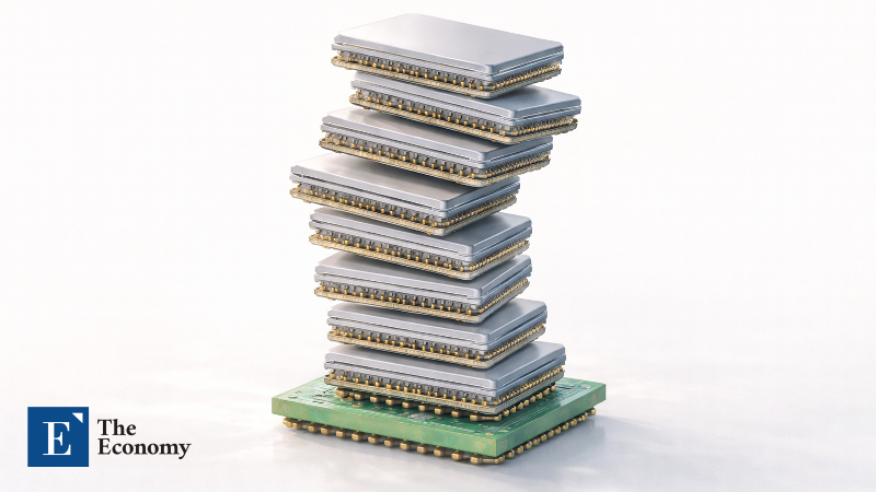
High-bandwidth flash (HBF) is also emerging as a next-generation memory semiconductor. HBF is built by stacking NAND flash rather than DRAM. While it does not process data as quickly as HBM, it can accommodate far more layers, making it suitable for reading and writing large-scale data. A 12-high fifth-generation HBM3E stack, for instance, offers only 36GB of capacity, whereas HBF products with more than 321 layers and a single-package capacity of 256GB are gradually moving toward commercialization.
HBM’s Fundamental Limitations
The rapid emergence of these new technologies reflects the extent to which AI has transformed the memory market environment. At present, major memory customers are demanding ultra-high-speed memory products. The exponential expansion of large language models (LLMs) has driven a steep increase in required bandwidth. In response, memory suppliers have moved to raise the processing speeds of advanced HBM products. Samsung Electronics has implemented data-transfer speeds of about 11.7Gbps per pin in sixth-generation HBM4, while SK hynix has secured operating speeds above 10Gbps and declared its readiness for mass production. Micron, for its part, has also achieved speeds exceeding 11Gbps on a sample basis.
The problem is that as HBM’s data-processing speed rises, the associated power burden increases sharply. HBM exchanges enormous volumes of data with GPUs on a second-by-second basis. In particular, in the latest HBM3E and HBM4 products, bandwidth per stack has expanded to around 2TB/s, multiplying data movement severalfold from earlier generations. As a result, memory stacks now account for a substantial share of the power budget within AI accelerator packages, while AI servers, where dozens of HBM units operate simultaneously, have seen a marked increase in total system-wide power consumption.
As AI models continue to advance rapidly, demands for higher memory performance will inevitably intensify. That means the performance of HBM, already associated with a considerable power burden, will have to be improved repeatedly going forward. For companies already constrained by soaring power and cooling costs at data centers, this could translate into additional cost pressure. That is why new memory architectures and alternative technologies with superior power efficiency are emerging across the industry.
Efforts to Advance Existing Technologies Remain Intact
At the same time, efforts to further advance HBM equipment, materials, and processes are still continuing. One example came on March 11, when U.S. semiconductor equipment manufacturer Applied Materials announced that it had signed a long-term technology collaboration agreement with SK hynix to develop next-generation memory for AI and high-performance computing. The core of the partnership is the joint pursuit of materials engineering and process innovation centered on next-generation DRAM and HBM technologies. Engineers from both companies are set to conduct joint research at the EPIC (Equipment and Process Innovation and Commercialization) Center being established in Silicon Valley, with research programs focused on discovering new materials, integrating complex processes, and advancing HBM-class advanced packaging technologies.
Hybrid bonding equipment has also entered the early stages of commercialization. The TC bonder currently used in HBM manufacturing employs a method of joining DRAM layers by inserting bumps that transmit electrical signals between them, enabling the production of HBM stacks of up to 16 layers. The issue is that as HBM performance becomes increasingly sophisticated, the number of DRAM layers in HBM products, currently at 12 and 16 layers, is highly likely to rise beyond 20. If TC bonder equipment is used to push DRAM stacking past 20 layers, overall thickness increases, potentially causing signal delay and greater power consumption.
Hybrid bonding emerged to overcome those limitations. It eliminates the bumps essential to TC bonders and directly bonds the DRAM layers together. That reduces the space between DRAM layers, allowing more DRAM to be stacked at the same height while also improving signal-transfer speed. Across the semiconductor industry, the prevailing view is that hybrid bonding will be commercialized starting with seventh- and eighth-generation HBM products, or HBM4E through HBM5, where stack counts are expected to exceed 20 layers.
Competition among memory suppliers in “customized HBM” has also intensified. Customized HBM is a product in which the base die, the substrate that serves as the “brain” of HBM, is designed to meet each customer’s specific requirements. Because it performs a range of computations tailored to customer needs, it is also referred to as computing in memory (CIM). One market expert explained, “The proprietary AI chips developed by global big-tech companies each require different levels of data-processing performance, power consumption, and thermal characteristics from HBM. Demand for customized products focused on optimizing the functions of each company’s AI chips, rather than standardized HBM, is bound to increase.”
Similar Post