Semiconductor Miniaturization Race Cools, as ‘Packaging’—Not the Chip—Begins to Decide Performance
Input
Modified
Packaging emerges as a key variable in the 2-nanometer race
Samsung touts “preemptive investment” vs. SK’s “cautious approach”
Taiwan’s overwhelming expansion raises latent risks for South Korea

The yardstick for semiconductor performance competition has been shifting. The industry has moved beyond an earlier phase that fixated on how much smaller chips could be made, and toward a new center of gravity: how finished chips can be connected and stacked to function as a single system. As advanced packaging moves to the heart of that transition, the 2-nanometer race among leading foundry players, including Samsung Electronics, appears set to be decided at this inflection point. With Samsung Electronics and SK hynix diverging in strategic direction and Taiwan pressing ahead with a major expansion of packaging bases, the competitive landscape has entered a phase that looks increasingly difficult to forecast.
Heat, Power, and Performance Converge in Integrated Design Competition
According to the IT outlet DigiTimes, the advanced packaging market—an advanced back-end semiconductor process—could grow to $80.5 billion by 2033. The pace would significantly outstrip overall semiconductor market growth, and the outlet reported that “as the 2-nanometer (nm) process becomes a reality, the axis of innovation has shifted from transistor scaling to chiplet assembly and advanced packaging.” It added that “system-level integrated design and packaging capabilities will differentiate the competitiveness of major foundry players such as Samsung Electronics, TSMC, and Intel.”
For years, the industry’s main competitive axis centered on placing more transistors within the same area—reducing linewidth to boost density. However, in the transition to 2 nm, performance gains have become limited, while costs for design, verification, and mass production have risen to levels exceeding $100 million. This implies that the pace of cost increases has become steeper than the pace of performance improvements as scaling advances. Even so, competition to mass-produce at 2 nm has been intensifying. Samsung Electronics plans to build a 2 nm wafer production system capable of 20,000 wafers per month within the year, while TSMC began volume production of its 2 nm process in the fourth quarter of last year.
At 2 nm, gate-all-around (GAA) structures replace conventional FinFETs. By expanding the contact interface between the gate and channel from three sides to four, the approach improves current control and enables lower-power operation. Samsung Electronics commercialized GAA first in the industry with its 3 nm process in 2022 and has signaled an upgraded 2 nm GAA process. TSMC attempted GAA for the first time with this 2 nm node, and has reportedly completed prototype development for existing customers.
Intel is pursuing a strategy of maximizing the combined effect of RibbonFET by applying backside power delivery (BSPDN) to its 18A process for the first time. Such process transitions are aimed at improving power efficiency, but they carry the limitation that power density also rises as density increases. AI and data center chips, in particular, run around the clock, which brings the requirement that thermal management and dynamic power monitoring must be built into the design from the earliest stages. The solution gaining prominence at this point has been advanced packaging.
Packaging refers to the back-end process that cuts a finished front-end wafer into individual chips, then protects, bonds, and connects them to electrically integrate them into a system. A protective film is first applied through lamination, wafer thickness is reduced via back grinding, and the wafer is cut using wafer saw. The dies are then attached to a substrate, and electrical connections are formed through wire bonding or flip-chip bonding. Finally, the package is protected from external shock and moisture by molding with epoxy resin, and is completed through marking and solder-ball mounting into a form that can connect to a system board.
The 2.5D and 3D stacking approaches and chiplet architectures used in AI accelerators symbolize this shift. Chiplets assemble smaller, function-specific dies into a single package rather than relying on one large monolithic chip, and their defining feature is the ability to combine dies made on different process nodes within the same package. The approach applies the most advanced node only to compute regions that require peak performance, while building the rest on mature nodes to manage cost and yield risk. Nvidia chips, which account for more than 80% of the AI semiconductor chip market, use the 2.5D packaging technology CoWoS (Chip-on-Wafer-on-Substrate).
Samsung Electronics and SK hynix Diverge on Next-Generation Technology Strategy
Since the early 2020s, Samsung Electronics has faced a wave of crisis narratives as it ceded some market share to rival SK hynix. Yet during this period, the industry moved away from a planar, scaling-centered contest and toward stacking chips vertically and completing performance at the package level. In response, Samsung Electronics devised a strategy to introduce three-dimensional technology across system semiconductors, memory, and packaging. The judgment reflected limits to sustaining performance gains through purely horizontal expansion, given that while planar structures based on existing processes favor current flow and circuit design, they cap the number of transistors that can be integrated on a single plane.
Samsung Electronics has moved to develop “3DSFET,” combining the 3D stacking concept with GAA introduced at sub-3 nm nodes. If conventional GAA constitutes a single-transistor structure, 3DSFET stacks that structure vertically to maximize both area efficiency and power performance. The challenge is that implementation requires precise formation of vertical patterns. To minimize inter-layer interference and separate power paths, it becomes necessary to secure high-aspect-ratio structures reliably, and this has pushed cryogenic etching technology into the spotlight. The technique forms a solid protective layer on the silicon surface to control etching direction, enabling vertical pattern formation while managing sidewall damage.
Samsung Electronics has reportedly tested equipment from both Lam Research and Tokyo Electron (TEL) to introduce cryogenic etching. An industry source familiar with the matter said Samsung Electronics has been placing weight on incorporating cryogenic etching, starting with V10, into the standard process for next-generation V-NAND. The source added that as cryogenic etching becomes more widely applicable not only in memory but also in logic semiconductors, it could be deployed for precise via etching for backside power connections and for controlling metal-to-metal interconnect patterns.
In contrast to Samsung Electronics’ aggressive approach, SK hynix has signaled a cautious posture toward expanding packaging. Lee Kang-wook, vice president in charge of package development at SK hynix, said at the ‘SEMICON Korea 2026’ AI Summit on the 11th that the company was “considering various issues” regarding possible entry into the packaging business. At the same time, he added that construction of the packaging fab under development in Indiana would proceed without disruption, and that SK hynix had already secured the market through its proprietary HBM2E packaging technology ‘MR-MUF’ for third-generation high-bandwidth memory (HBM). This has been read as SK hynix placing greater weight on deepening memory-centered packaging built around HBM.

Taiwan Strengthens an Integrated Foundry–Packaging Ecosystem
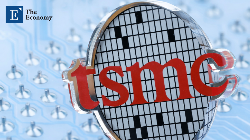
TSMC’s aggressive expansion strategy has also emerged as a key point to watch. TSMC is pursuing a plan to build the world’s largest cutting-edge packaging base on an 89.58-hectare site in Taibao City, Chiayi County, in southwestern Taiwan. The facility, built around 3D SoIC (System on Integrated Chip), is expected to incorporate heterogeneous packaging and apply it to AI, sixth-generation communications, cybersecurity, and quantum technologies. SoIC is TSMC’s 3D heterogeneous integration technology that stacks multiple chips vertically to raise both performance and power efficiency. Construction is expected to begin in the first half of this year, with completion as early as 2031.
TSMC is already building two packaging plants in a nearby science park, and if this expansion proceeds as planned, the structure would add plants three through five (P3–P5). TSMC expects the expansion to generate $6.666 billion in induced production effects and create 3,500 jobs. It also calculates that the project will contribute to forming an industrial cluster in southern Taiwan as a core hub for its high-performance computing (HPC) and AI chip strategy, a signal of reinforced domestic investment that can be read as directly countering concerns raised in some quarters about a weakening “silicon shield.”
In a report last year, Boston Consulting Group (BCG) assessed that “South Korea’s chances of gaining an advantage in the packaging revolution remain very slim for now,” noting that Taiwan accounts for five of the world’s top 10 packaging companies while South Korea accounts for none. The report argued that while South Korea’s HBM has secured technological leadership, advanced packaging that attaches HBM to AI semiconductors is largely carried out in Taiwan. South Korean government data similarly showed Samsung Electronics and SK hynix relying on overseas sources for more than 95% of key materials and equipment for advanced packaging.
Industry participants have said the gap reflects differences in ecosystem structure. Kim Nam-seok, CEO of LB Semicon, said, “Packaging forces you to accelerate development even before securing customers, and it is hard for a mid-sized company to bear the risk alone.” Choi Bong-seok, author of the book Hidden Giants of the Semiconductor Industry, also said, “Taiwan has the world’s top packaging company ASE, and even smaller firms have dozens of customers, while domestic packaging firms depend on a single customer for 70% to 90% of revenue.” This has fed an assessment that, unlike Taiwan, which strengthened a horizontally collaborative ecosystem, South Korea has remained within memory-centered vertical integration.
Reshaping of the global supply chain has also been cited as a variable. The United States has been pursuing policies to bring advanced packaging technology onshore, and SK hynix said it plans to invest $3.87 billion in R&D collaboration with Purdue University. At the same time, the shift of commodity packaging capacity to Southeast Asia has been accelerating. Intel plans to operate packaging facilities in Penang, Malaysia, with an investment of $7 billion, and the Malaysian government also announced a $5.3 billion investment plan while declaring an initiative to train 60,000 semiconductor engineers. With large-scale bases concentrated in Taiwan, cutting-edge capabilities pulled toward the United States, and traditional volume distributed across Southeast Asia, the broader industry view has been that South Korea’s packaging industry faces a pivotal strategic decision point.


Comment