Pushing Ahead With “Terafab” While Coordinating With Samsung? The Two Pillars of Tesla’s Semiconductor Strategy

Authored On
Modified
Supply chain independence exposed amid a cooperative framework
Securing confidence in advanced 2-nanometer yield remains a challenge
TSMC’s dominance in the foundry market continues
Tesla is drawing industry attention with a dual-track approach to semiconductor procurement. While entrusting Samsung Electronics with large-scale production of artificial intelligence (AI) chips, it is simultaneously signaling its determination to build supply chain independence through its own manufacturing base. The structure reflects the parallel operation of two imperatives: the short-term need for rapid mass production and the long-term strategy of securing semiconductors directly.
Attempt to build a self-sufficient semiconductor system
On the 26th, IT publication DigiTimes reported that “Tesla is shifting its strategic center of gravity away from a costly independent manufacturing approach and toward securing Samsung Electronics’ production capacity while jointly addressing chronic yield issues.” As Elon Musk has identified Austin, Texas, as the site for “Terafab,” an integrated semiconductor manufacturing base, the report suggested that close coordination with Samsung Electronics’ Taylor foundry plant, located nearby, is likely.
Musk’s Terafab concept is a vertically integrated model encompassing design, production, and packaging. It aims to secure 1 terawatt of annual computing power, with investment projected to reach as much as $60 billion. However, given that semiconductor fab construction and equipment installation typically require more than three years, there are clear time constraints on bringing mass production forward through Tesla’s own efforts alone. That means that despite its ambitions for semiconductor self-sufficiency, Tesla cannot forgo cooperation with existing foundries in the near term.
The scenario of coordination with Samsung Electronics emerged as a solution to this reality. Samsung’s Taylor plant, which is being built at a cost of $44 billion, is more than 90% complete and is located about 40 minutes by car from the Seaholm Power Plant site in Austin, where Terafab is planned. These conditions improve efficiency from both logistics and collaboration standpoints. Industry observers believe Tesla is likely to secure early production volumes by effectively using Samsung’s infrastructure as a dedicated manufacturing base. Tesla also laid the groundwork for such cooperation by signing a $16.5 billion AI chip supply agreement with Samsung Electronics in the second half of last year.
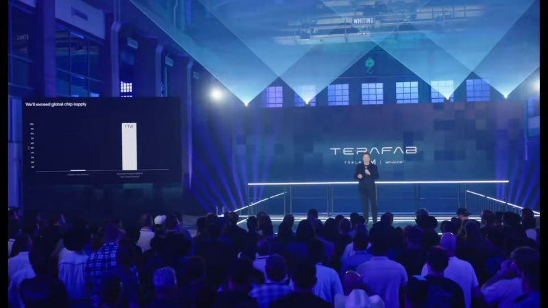
Even so, Musk’s emphasis on direct production reflects deep concern over supply shortages. At the Terafab project launch event on the 22nd, he said, “The market’s current semiconductor supply capacity amounts to only about 2% of what Tesla, SpaceX, and xAI need,” arguing that the pace of capacity expansion by existing manufacturers is failing to keep up with demand growth. Bloomberg also described Musk’s Terafab plan as “extraordinary in scale,” calling it “a clear indication of the severity of the semiconductor supply shortage.”

Samsung pushes hard for yield stabilization
At the same time, Samsung Electronics is struggling to raise yields on its 2-nanometer process. According to industry sources, Samsung’s 2-nanometer yield has risen to above 60% in some cases. Compared with the 20% range in the second half of last year, that marks an improvement of more than threefold in roughly two quarters. Yield refers to the share of properly functioning chips among all chips produced from a single wafer, meaning a 60% yield implies that only 60 out of 100 chips qualify as good products. Because advanced nodes carry a higher risk of process deviations and defects, rising yields are interpreted as a sign that technological stabilization has reached a certain level.
Even so, by absolute standards, Samsung still has ground to make up. While rival TSMC is believed to have achieved roughly 70% yield on its 2-nanometer process, Samsung has surpassed 60% in some product categories, but average yields for its smartphone chip Exynos 2600 remain below 50%. The 2-nanometer node features extremely high circuit density, which significantly increases the probability of defects caused by process variability. As a result, even under the same process, yield disparities can widen substantially depending on product type and design structure, making it difficult to secure large orders from major customers.
Yield is also directly tied to cost structure. The higher the number of good chips produced from one wafer, the lower the manufacturing cost per chip. Conversely, when yields are low, more wafers and process time are required to secure the same output, causing costs to rise sharply. For that reason, foundry businesses can face limits on order intake if yields fail to exceed a certain threshold. Samsung is therefore accumulating 2-nanometer process experience through orders from its own System LSI division as well as from China’s Canaan and MicroBT. The strategy is interpreted as one of first raising yields on relatively simple products before expanding to more complex chips.
The market sees crossing the 70% yield threshold at 2 nanometers as a decisive inflection point. Achieving that level would likely lead to orders from major customers such as Qualcomm and AMD, while failing to do so could delay the turnaround of Samsung’s non-memory business into profitability through expanded orders. While continuing development of its next-generation 1.4-nanometer process, Samsung plans to focus for now on optimizing 2-nanometer production. That is read as a judgment to prioritize yield stability and raise actual manufacturing competitiveness rather than forcing its technology roadmap forward too aggressively.
Will Tesla become a “third player”?
Viewed across the foundry industry as a whole, the current competitive structure resembles a TSMC-centered near-monopoly. According to market research firm TrendForce, revenue at the world’s top 10 foundry companies rose 26.3% year over year to a record $169.5 billion last year. Of that total, TSMC accounted for $122.5 billion in revenue and a dominant 69.9% market share. Samsung Electronics, by contrast, posted $12.6 billion in revenue and a 7.2% share. The gap in market share between the two widened from 55 percentage points in 2024 to 62.7 percentage points in just one year.
The problem is the market imbalance that such one-sided dominance can produce. TrendForce expects global foundry revenue to rise another 24.8% this year to $218.8 billion. At the center of that growth is demand for AI semiconductors. As Nvidia and AMD GPUs, along with custom chip development by North American cloud service providers such as Google, Amazon Web Services, and Meta, accelerate, demand for advanced 4-nanometer and sub-4-nanometer processes is expanding rapidly. With supply continuing to lag demand, reliance on a single foundry is increasingly being viewed as a risk.
That is also why Tesla has made an unusual semiconductor push outside its traditional business path. The company appears to have concluded that relying solely on existing foundries will not be sufficient to meet expanding semiconductor demand tied to autonomous driving, robotics, and AI data centers. By lowering dependence on any one supplier and securing the option to switch to in-house production if necessary, Tesla may be seeking greater leverage in price and volume negotiations. Even so, the prevailing view is that building an independent manufacturing system in the short term will be difficult, given the challenges of semiconductor production know-how, large-scale capital investment, and securing equipment supply chains.
Similar Post